JMSH0401AGQ规格参数 |
|||
|---|---|---|---|
| Type | 汽车MOSFET | ||
| RoHS | |||
| 制造商 | JJM | ||
| 类型 | N | ||
| VDS_Max/V | 40 | ||
| ID_Max /A | 197 | ||
| VGS(th)Typ/V | 2.8 | ||
| RDS(ON)Typ (mΩ)@ VGS 10V | 1.3 | ||
| RDS(ON)Max (mΩ)@ VGS 10V | 1.7 | ||
| VGS_Max/V | ±20 | ||
JMSH0401AGQ详情
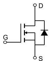
40V 1.3mΩ N通道功率MOSFET
JMSH0401AGQ特点
- 超低导通电阻,
- 低栅极电荷,
- 100% UIS 和 测试
- 无铅镀层
- 无卤素且符合 RoHS 标准
- 符合 AEC-Q101 标准,适用于汽车应用
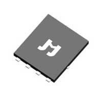
 PDFN5x6-8L
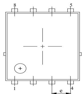
 底部视图
底部视图
JMSH0401AGQ产品概要
| Parameter | Value | Unit |
| VDS | 40 | V |
| VGS(th)_Typ | 2.8 | V |
| ID (@ VGS = 10V) (1) | 197 | A |
| RDS(ON)_Typ (@ VGS = 10V) | 1.3 | mΩ |
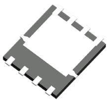
 Top View
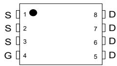
 Pin Configuration
JMSH0401AGQ订购信息
| Device | Package | # of Pins | Marking | MSL | TJ(°C) | Media | Quantity (pcs) |
| JMSH0401AGQ-13 | PDFN5x6-8L | 8 | SH0401AQ | 1 | -55 to 175 | 13-inch Reel | 5000 |
Absolute Maximum Ratings (@unless otherwise specified)
| Parameter | Symbol | Value | Unit | |
| Drain-to-Source Voltage | VDS | 40 | V | |
| Gate-to-Source Voltage | VGS | ±20 | V | |
| Continuous Drain Current (1) | TC=25°C | ID | 197 | A |
| TC=100°C | 139 | |||
| Pulsed Drain Current (2) | IDM | 748 | A | |
| Avalanche Current (3) | IAS | 36 | A | |
| Avalanche Energy (3) | EAS | 194 | mJ | |
| Power Dissipation (4) | TC=25°C | PD | 136 | W |
| TC=100°C | 68 | |||
| Junction & Storage Temperature Range | TJ, TSTG | -55 to 175 | °C | |
 vs.
vs.
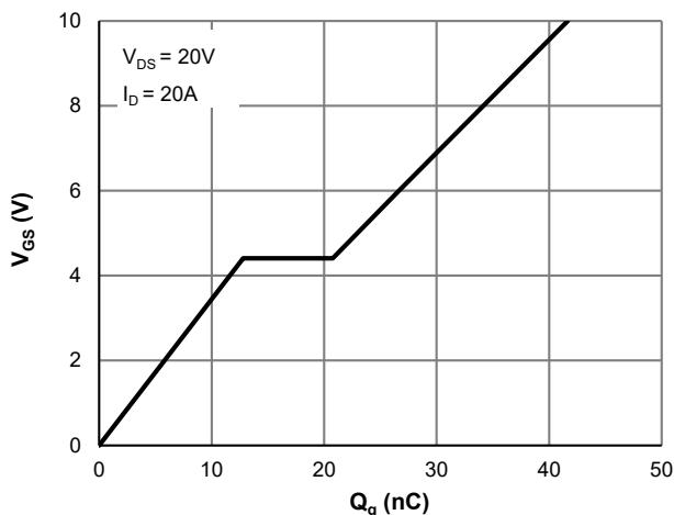 Gate Charge
JMSH0401AGQ电气特性 (@unless otherwise specified)
| Parameter | Symbol | Conditions | Min. | Typ. | Max. | Unit | |
| STATIC PARAMETERS | |||||||
| Drain-Source Breakdown Voltage | V(BR)DSS | ID=250μA, VGS=0V | 40 | V | |||
| Zero Gate Voltage Drain Current | IDSS | VDS=32V, VGS=0V | 1.0 | μA | |||
| TJ=55°C | 5.0 | ||||||
| Gate-Body Leakage Current | IGSS | VDS=0V, VGS=±20V | ±100 | nA | |||
| Gate Threshold Voltage | VGS(th) | VDS=VGS, ID=250μA | 2.2 | 2.8 | 3.4 | V | |
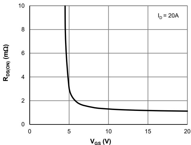
| Static Drain-Source ON-Resistance | RDS(ON) | VGS=10V, ID=20A | 1.3 | 1.7 | mΩ | ||
| Forward Transconductance | gFS | VDS=5V, ID=20A | 90 | S | |||
| Diode Forward Voltage | VSD | IS=1A, VGS=0V | 0.68 | 1.0 | V | ||
| Diode Continuous Current | IS | TC=25°C | 197 | A | |||
动态参数 (5)
| Input Capacitance | Ciss | VGS=0V, VDS=20V, f=1MHz | 3015 | pF | ||
| Output Capacitance | Coss | 2000 | pF | |||
| Reverse Transfer Capacitance | Crss | 18.0 | pF | |||
| Gate Resistance | Rg | VGS=0V, VDS=0V, f=1MHz | 3.0 | Ω |
切换参数 (5)
| Total Gate Charge (@ VGS = 10V) | Qg | VGS= 0 to 10V VDS= 20V, ID= 20A | 42 | nC | ||
| Total Gate Charge (@ VGS = 6.0V) | Qg | 27 | nC | |||
| Gate Source Charge | Qgs | 12.8 | nC | |||
| Gate Drain Charge | Qgd | 8.0 | nC | |||
| Turn-On DelayTime | tD(on) | VGS= 10V, VDS= 20V RL= 1.0Ω, RGEN= 6Ω | 16.0 | ns | ||
| Turn-On Rise Time | tr | 20 | ns | |||
| Turn-Off DelayTime | tD(off) | 51 | ns | |||
| Turn-Off Fall Time | tf | 27 | ns | |||
| Body Diode Reverse Recovery Time | trr | IF= 20A, dIF/dt = 100A/μs | 49 | ns | ||
| Body Diode Reverse Recovery Charge | Qrr | IF= 20A, dIF/dt = 100A/μs | 44 | nC |
JMSH0401AGQ热特性
| Parameter | Symbol | Typ. | Max. | Unit |
| Thermal Resistance, Junction-to-Ambient | RθJA | 48 | 57 | °C/W |
| Thermal Resistance, Junction-to-Case | RθJC | 1.1 | 1.3 | °C/W |
备注
- 计算的连续电流假设条件为而实际连续电流取决于热和 机电应用板设计。
- 该单脉冲测量是在
- 该单脉冲测量是在以下情况下进行的 条件而其值受.
- 功耗基于.
- 此值由设计保证,因此不包含在 生产测试。
JMSH0401AGQ典型电气和热特性
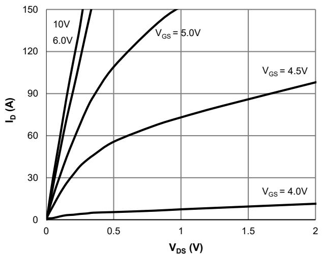 Figure 1: Saturation Characteristics
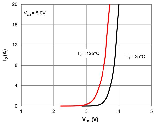 Figure 2: Transfer Characteristics
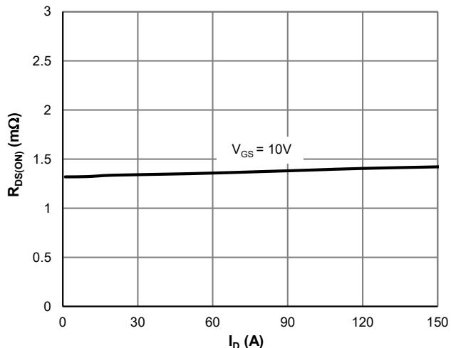 Figure 3:vs.Drain Current
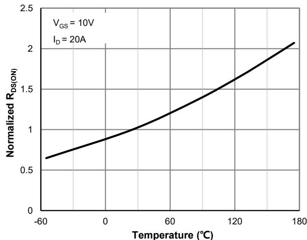 Figure 4:vs.Junction Temperature
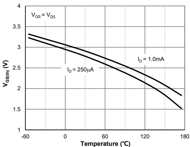 Figure 5:vs.Junction Temperature
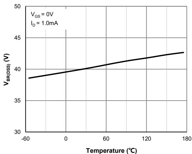 Figure 6:vs.Junction Temperature
Typical Electrical & Thermal Characteristics
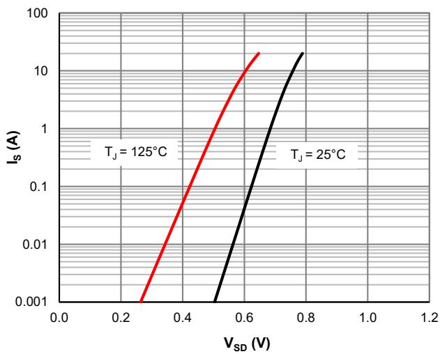 Figure 7: Body-Diode Characteristics
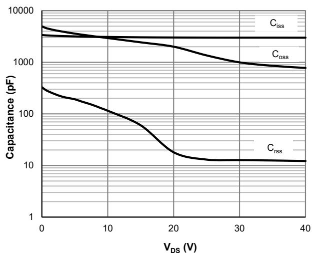 Figure 8: Capacitance Characteristics
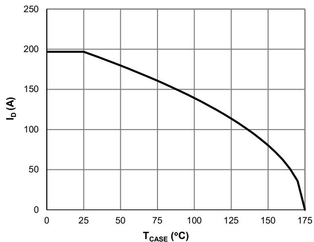 Figure 9: Current De-rating
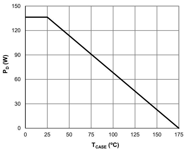 Figure 10: Power De-rating
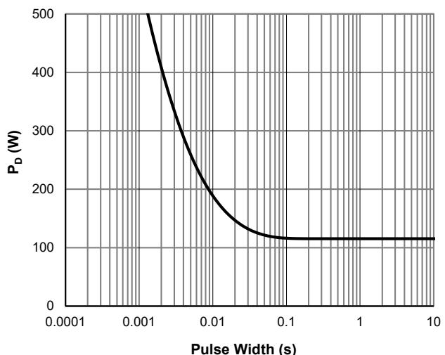 Figure 11: Single Pulse Power Rating, Junction-to-Case
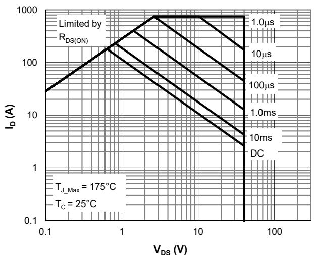 Figure 12: Maximum Safe Operating Area
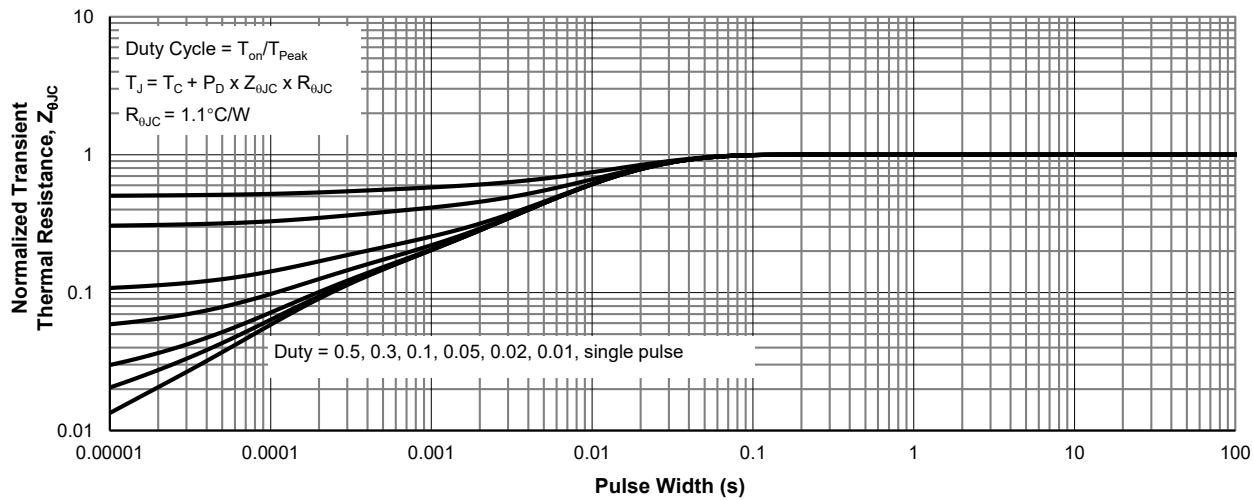 Figure 13: Normalized Maximum Transient Thermal Impedance
PDFN5x6-8L 封装信息
 Package OutlineTop View
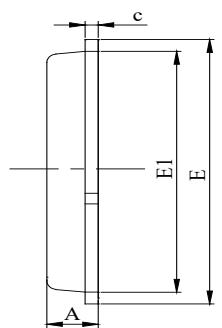 Side View
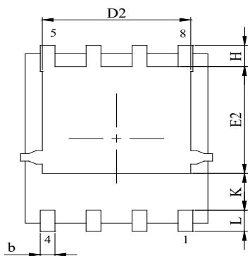 Bottom View
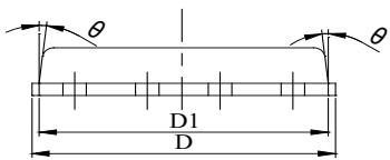 Front View
NOTES:
- Dimension and tolerance per ASME Y14.5M, 1994.
- All dimensions in millimeter (angle in degree).
- Dimensions D1 and E1 do not include mold flash protrusions or gate burrs.
| DIM. | MILLIMETER | ||
| MIN. | NOM. | MAX. | |
| A | 0.90 | 1.00 | 1.10 |
| b | 0.31 | 0.41 | 0.51 |
| c | 0.20 | 0.25 | 0.30 |
| D | 5.00 | 5.20 | 5.40 |
| D1 | 4.95 | 5.05 | 5.15 |
| D2 | 4.00 | 4.10 | 4.20 |
| E | 6.05 | 6.15 | 6.25 |
| E1 | 5.50 | 5.60 | 5.70 |
| E2 | 3.42 | 3.53 | 3.63 |
| e | 1.27BSC | ||
| H | 0.60 | 0.70 | 0.80 |
| L | 0.50 | 0.70 | 0.80 |
| K | 1.23 REF | ||
| θ | - | - | 10° |
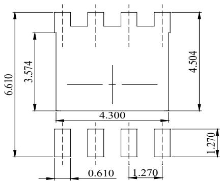 Recommended Soldering FootprintDIMENSIONS:MILLIMETERS