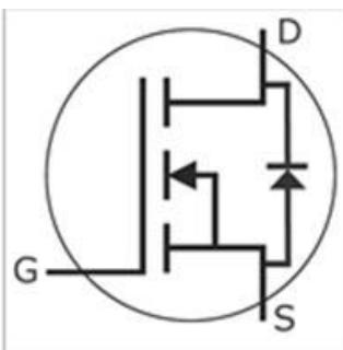
制造商
厂商型号
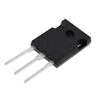
封装
规格书
描述
LGE3M650170B规格参数 |
|||
|---|---|---|---|
| Type | 碳化硅MOSFET | ||
| RoHS | |||
| 制造商 | LGE | ||
| VDS/V | 1700 | ||
| ID/A | 7 | ||
| RDS/mΩ | 650 | ||
| PD/W | 62 | ||
LGE3M650170B详情
LGE3M650170B特征
高阻断电压,低导通电阻
低电容的高速开关
- 易于并联和驱动
- 超低漏栅电容
LGE3M650170B优点
更高的系统效率
降低冷却要求
- 提高系统可靠性
- 提高系统开关频率
LGE3M650170B应用
- 辅助电源
- 开关模式电源
- 高压电容式

| Part Number | Package | Marking |
| LGE3M650170B | TO-247-3 | LGE3M650170B |
Maximum Ratings unless otherwise specified)
| Symbol | Parameter | Value | Unit | Test Conditions | Note |
| VDSmax | Drain-Source Voltage | 1700 | V | VGS=0V, ID=100μA | |
| VGSmax | Gate-Source Voltage | -10/+25 | V | Absolute maximum values | |
| VGSop | Gate-Source Voltage | -5/+20 | V | Recommended operational values | |
| ID | Continuous Drain Current | 7.0 | A | VGS=20V, Tc=25°C | |
| 4.5 | VGS=20V, Tc=100°C | ||||
| ID(pulse) | Pulsed Drain Current | 9.0 | A | Pulse width tp limited by TJmax | |
| PD | Power Dissipation | 62 | W | Tc=25°C, TJ=150°C | |
| TJ, TSTG | Operating Junction and Storage Temperature | -55 to +150 | °C |
Caution: This device is sensitive to electrostatic discharge .Users should follow ESD handing procedures.
Electrical Characteristics unless otherwise specified)
| Symbol | Parameter | Min. | Typ. | Max. | Unit | Test Conditions | Note |
| V(BR)DSS | Drain-Source Breakdown Voltage | 1700 | / | / | V | VGS=0V, ID=100μA | |
| VGS(th) | Gate Threshold Voltage | 2.0 | 2.6 | 4.0 | V | VDS=VGS, ID=1.0mA | Fig. 11 |
| / | 1.8 | / | VDS=VGS, ID=1.0mA, TJ=150°C | ||||
| IDSS | Zero Gate Voltage Drain Current | / | 1 | 100 | μA | VDS=1700V, VGS=0V | |
| IGSS+ | Gate-Source Leakage Current | / | 10 | 250 | nA | VDS=0V, VGS=25V | |
| IGSS- | Gate-Source Leakage Current | / | 10 | 250 | nA | VDS=0V, VGS=-10V | |
| RDS(on) | Drain-Source On-State Resistance | / | 650 | 850 | mΩ | VGS=20V, ID=2.0A | |
| / | 1300 | / | VGS=20V, ID=2.0A, TJ=150°C | ||||
| gfs | Transconductance | / | 1.06 | / | S | VDS=20 V, ID=2.0 A | Fig. 4,5,6 |
| / | 1.14 | / | VDS=20V, ID=2.0A, TJ=150°C | ||||
| Ciss | Input Capacitance | / | 194 | / | pF | VGS=0V | Fig. 15,16 |
| Coss | Output Capacitance | / | 13 | / | VDS=1000V | ||
| Crss | Reverse Transfer Capacitance | / | 1.8 | / | f=1MHz | ||
| Eoss | CossStored Energy | / | 6.6 | / | μJ | VAC=25mV | |
| EON | Turn-On Switching Energy | / | 5 | / | mJ | VDS=1200V, VGS=-5V/20V | |
| EOFF | Turn-Off Switching Energy | / | 9.2 | / | ID=2.0A, RG(ext)=2.5Ω, L=100μH | ||
| td(on) | Turn-On Delay Time | / | 13.8 | / | ns | VDS=1200V, VGS=-5V/20V, ID=2.0ARG(ext)=2.5Ω, RL=20Ω | |
| tr | Rise Time | / | 22.8 | / | |||
| td(off) | Turn-Off Delay Time | / | 38 | / | |||
| tf | Fall Time | / | 14 | / | |||
| RG(int) | Internal Gate Resistance | / | 18 | / | Ω | f=1MHz, VAC=25mV | |
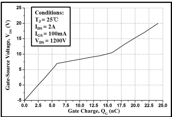
| QGS | Gate to Source Charge | / | 5.4 | / | nC | VDS=1200V | |
| QGD | Gate to Drain Charge | / | 7.6 | / | VGS=-5V/20V | ||
| QG | Total Gate Charge | / | 23 | / | ID=2.0A |
Reverse Diode Characteristics
| Symbol | Parameter | Typ. | Max. | Unit | Test Conditions | Note |
| VSD | Diode Forward Voltage | 4.2 | / | V | VGS=-5V, ISD=25A | Fig. 8,9,10 |
| 3.9 | / | VGS=-5V, ISD=25A, TJ=150°C | ||||
| IS | Continuous Diode Forward Current | / | 7.0 | A | TC=25°C | |
| trr | Reverse Recover Time | 25 | / | ns | VR=1200V, ISD=2.0A | |
| Qrr | Reverse Recovery Charge | 15 | / | nC | ||
| Irrm | Peak Reverse Recovery Current | 2.8 | / | A |
Thermal Characteristics
| Symbol | Parameter | Typ. | Max. | Unit | Test Conditions | Note |
| RθJC | Thermal Resistance from Junction to Case | 1.8 | / | °C/W | ||
| RθJA | Thermal Resistance from Junction to Ambient | / | 40 |
Caution: This device is sensitive to electrostatic discharge .Users should follow ESD handing procedures.
LGE3M650170B典型性能
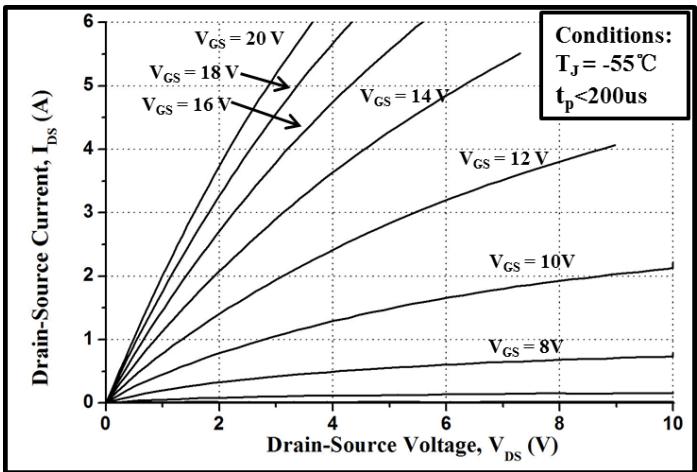
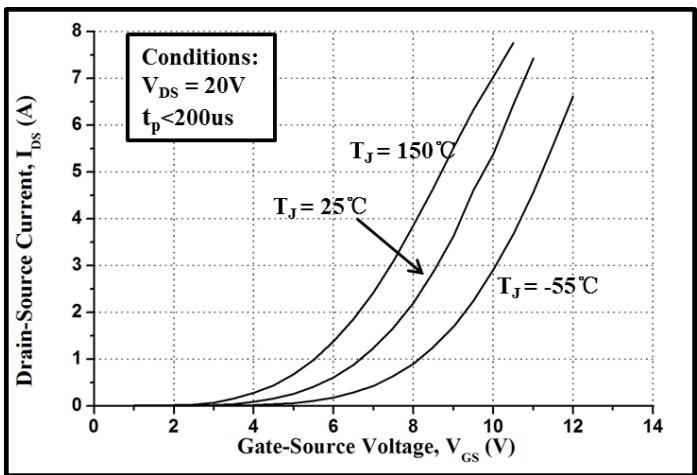
Figure 1. Output Characteristics
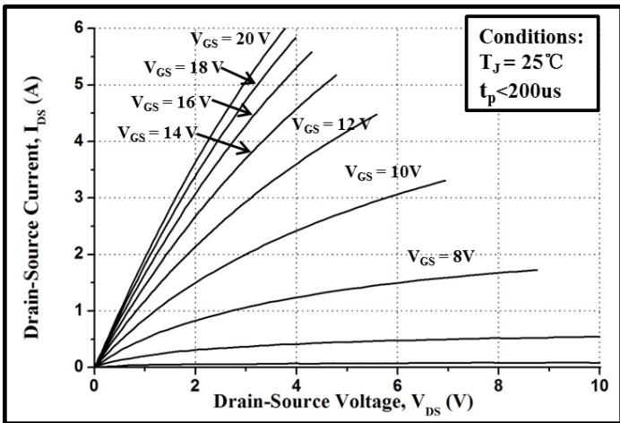
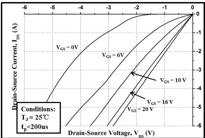
Figure 2. Output Characteristics
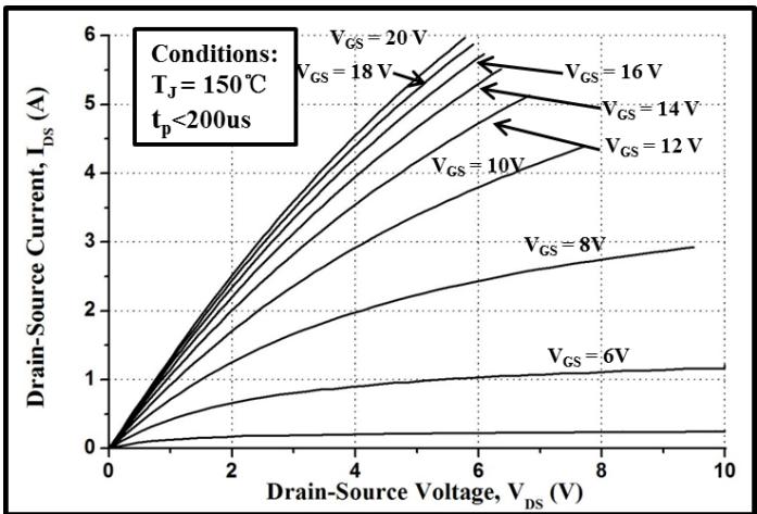
Figure 3. Output Characteristics
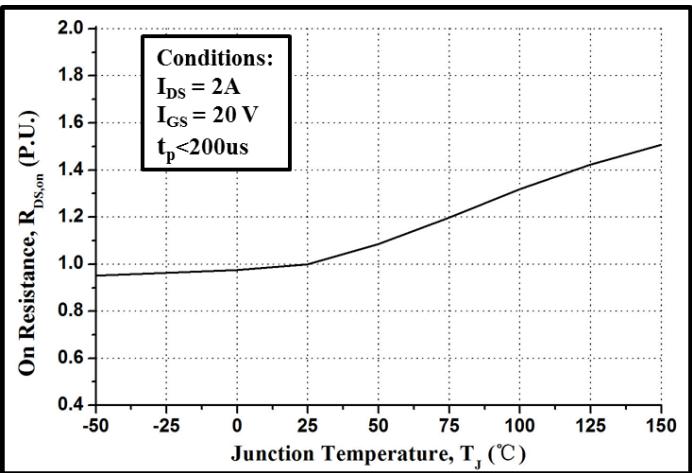
Figure 4. Normalized On-Resistance vs. Temperature
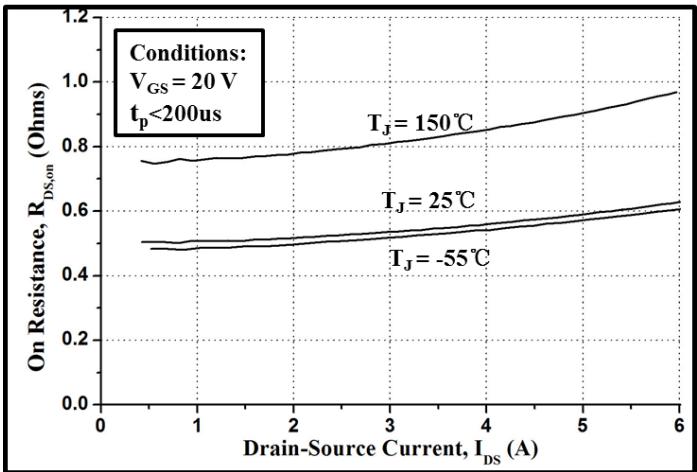
Figure 5. On-Resistance vs. Drain Current For Various Temperatures
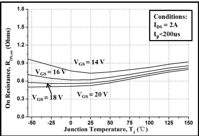
Figure 6. On-Resistance vs. Temperature For Various Gate Voltage
Caution: This device is sensitive to electrostatic discharge .Users should follow ESD handing procedures.
Typical Performance
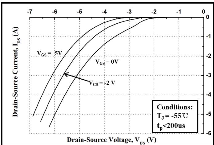
Figure 8. Body Diode Characteristic at
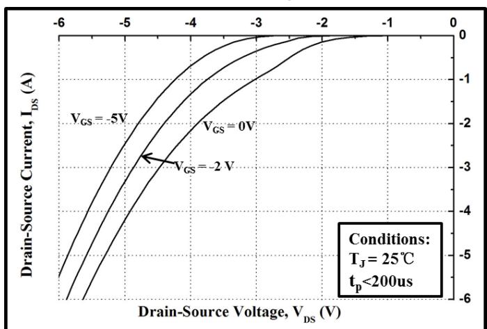
Figure 7. Transfer Characteristic for Various Junction Temperatures
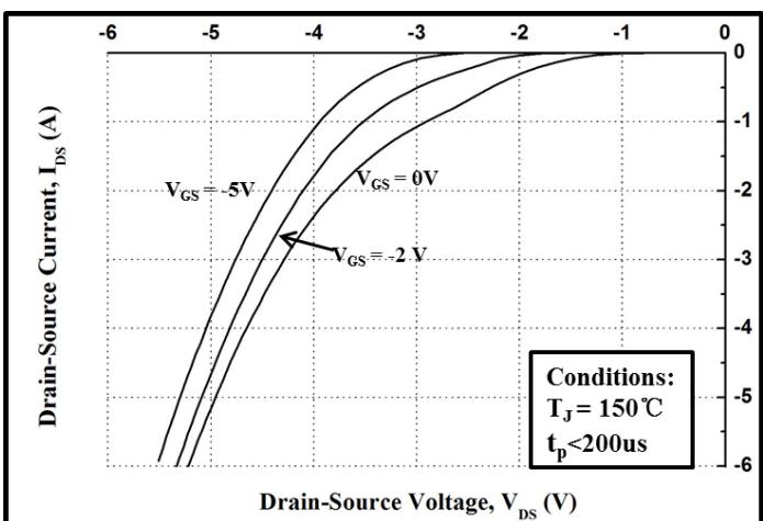
Figure 10. Body Diode Characteristic at
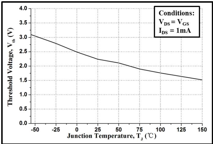
Figure 9. Body Diode Characteristic at
Figure 11. Threshold Voltage vs. Temperature
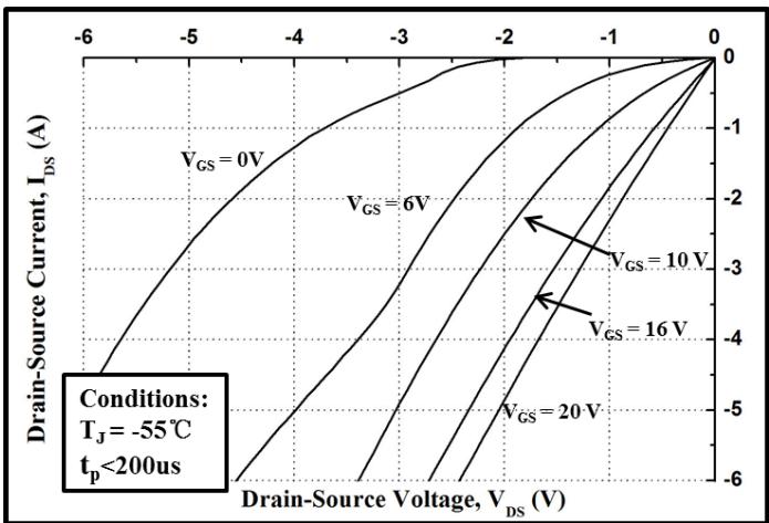
Figure 12. 3rd Quadrant Characteristic at
Caution: This device is sensitive to electrostatic discharge .Users should follow ESD handing procedures.
Typical Performance
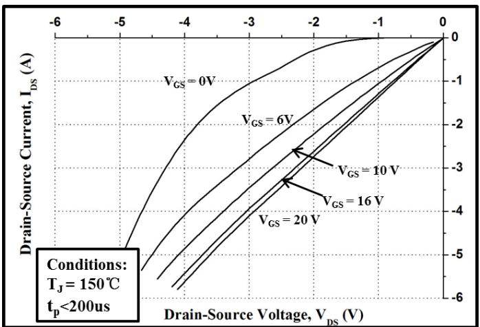
Figure 14. 3rd Quadrant Characteristic at
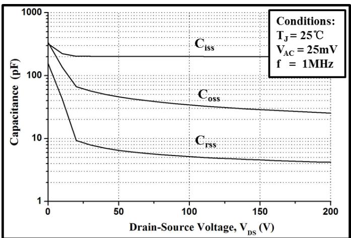
Figure 13. 3rd Quadrant Characteristic at
Figure 15. Capacitances vs. Drain-Source
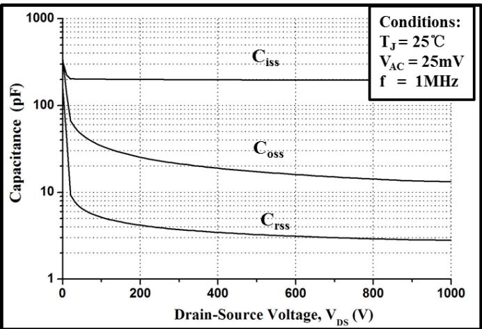
Figure 16. Capacitances vs. Drain-Source
Voltage (0 - 200V)
Figure 17. Gate Charge Characteristic
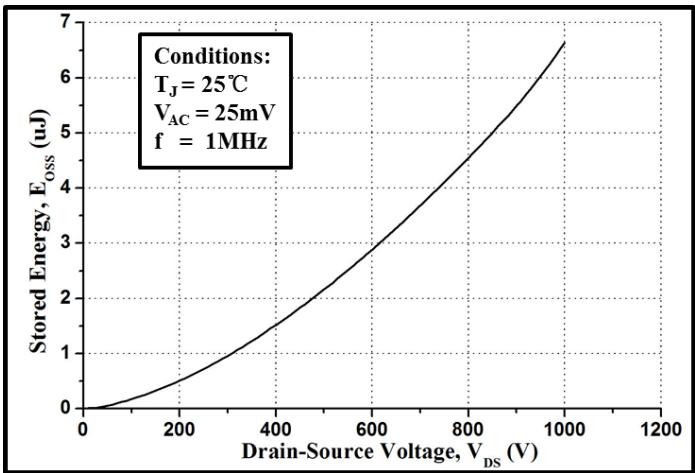
Figure 18. Output Capacitor Stored Energy
Caution: This device is sensitive to electrostatic discharge .Users should follow ESD handing procedures.
LGE3M650170B包装尺寸
Package TO-247-3
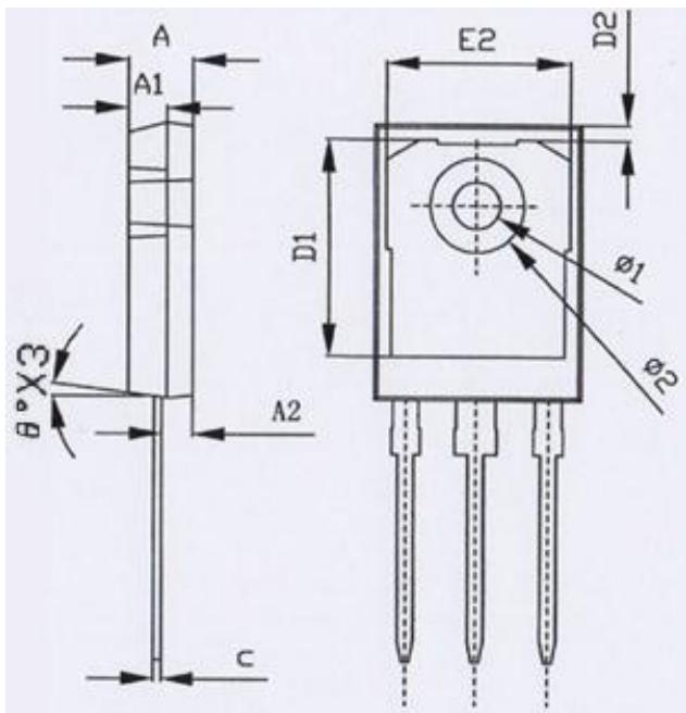
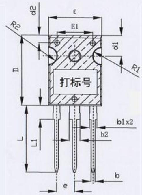
| SYMBOLS | DIMENSIONS IN MILLMETERS | ||
| MIN | NOM | MAX | |
| A | 4.9 | 5 | 5.1 |
| A1 | 2.9 | 3 | 3.1 |
| A2 | 2.31 | 2.36 | 2.41 |
| b | 1.16 | 1.2 | 1.26 |
| b1 | 2.05 | - | 2.2 |
| b2 | 3.05 | - | 3.2 |
| c | 0.58 | 0.6 | 0.66 |
| D | 20.9 | 21 | 21.1 |
| D1 | 16.46 | 16.56 | 16.76 |
| D2 | 1.17 | ||
| d1 | 6.05 | 6.15 | 6.25 |
| d2 | 2.2 | 2.3 | 2.4 |
| E | 15.7 | 15.8 | 15.9 |
| E1 | 10.5 | ||
| E2 | 14.02 | ||
| e | - | 1.27bps | - |
| L | 19.82 | 19.92 | 20.02 |
| L1 | 1.88 | 1.98 | 2.08 |
| θ | 0° | 7° | 8° |
| R1 | - | 2.7 | - |
| R2 | - | 2.5 | - |
| Φ1 | 3.6 | ||
| Φ2 | - | 7.19 | - |
| Packge | Packing | Box Size L×W×H(mm) | Quantity(pcs/box) | Carton Size L×W×H(mm) | Quantity(pcs/carton) |
| TO-247 | 30pcs/Tube | 570×155×50 | 450 | 580×340×125 | 1800 |
警告:此设备对静电放电敏感。用户应遵循ESD处理程序。