JOC341规格参数 |
|||
|---|---|---|---|
| Type | 栅极驱动光耦合器 | ||
| RoHS | |||
| 制造商 | JJM | ||
| 输出IO/A | 3 | ||
| ICCH/L_Max/mA | 3 | ||
| VCC/V | 15 ~ 30 | ||
| 延迟TPHL_Max /ns | 110 | ||
| 延迟TPLH_Max /ns | 110 | ||
| 抗干扰CMH/L_Min /kV/μs | 20 | ||
| 隔离值VISO/VRMS | 5000 | ||
JOC341详情
JOC341系列光耦合器
3.0安培栅极驱动光耦
JOC341系列光耦合器非常适合驱动功率 用于电机控制逆变器应用的IGBT(和MOSFET)和 电源系统中的逆变器。它包含一个光学耦合的LED装置 连接到带有功率输出级的集成电路。
3.0A峰值输出电流可直接驱动大多数 IGBTs。对于评级更高的 IGBT,可以使用 JOC341 系列 驱动一个独立功率级,驱动IGBT门。
光耦合器的工作参数保证在 温度范围为 -.
JOC341特点
- 3.0 A最大峰值输出电流
- 轨对轨输出电压 - 最大传播延迟 110纳秒
- 在电压锁定保护(UVLO)带滞后保护下
- 宽工作范围:15至30伏
- 保证温度下的性能.
JOC341应用
- IGBT/MOSFET 栅极驱动
- 不间断电源(UPS) - 工业逆变器
- 交流/无刷直流电机驱动
- 切换电源
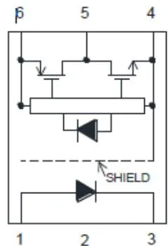
SCHEMATIC
引脚定义
4.VSS
1.Anode 5.VO
3.Cathode 6.VCC
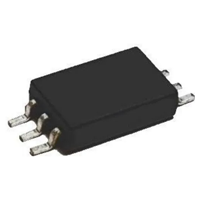
PACKAGE
真值表
| LED | VCC-VSS(Turn-ON,+ve going) | VCC-VSS(Turn-OFF,-ve going) | Vo |
| OFF | 0 - 30 V | 0 - 30 V | Low |
| ON | 0 - 11.0 V | 0 - 9.5 V | Low |
| ON | 11.0 - 13.5 V | 9.5 - 12 V | Transition |
| ON | 13.5 - 30 V | 12 - 30 V | High |
Note: A bypass capacitor must be connected between Pin 4 and 6.
绝对最大额定值
| PARAMETER | SYMBOL | Min | Max | UNIT | Note |
| Storage Temperature | Tstg | -55 | 125 | °C | - |
| Operating Temperature | Topr | -40 | 110 | °C | - |
| Output IC Junction Temperature | TJ | - | 125 | °C | - |
| Total Output Supply Voltage | (Vcc-Vss) | 0 | 35 | V | - |
| Average Forward Input Current | IF | - | 20 | mA | - |
| Reverse Input Voltage | VR | - | 5 | V | - |
| “High” Peak Output Current | IOH(PEAK) | 3.0 | A | 1 | |
| “Low” Peak Output Current | IOL(PEAK) | 3.0 | A | 1 | |
| Output Voltage | VO(PEAK) | -0.5 | Vcc | V | - |
| Power Dissipation | P1 | - | 45 | mW | - |
| Output IC Power Dissipation | Po | - | 700 | mW | - |
| Lead Solder Temperature | Tsol | - | 260 | °C | - |
Note: Ambient temperature = , unless otherwise specified. Stresses exceeding the absolute maximum ratings can cause permanent damage to the device. Exposure to absolute maximum ratings for long periods of time can adversely affect reliability.
Note 1: Exponential waveform. Pulse width
RECOMMENDED OPERATION CONDITIONS
| PARAMETER | SYMBOL | MIN. | MAX. | UNIT |
| Operating Temperature | TA | -40 | 110 | °C |
| Supply Voltage | VCC | 15 | 30 | V |
| Input Current (ON) | IF(ON) | 7 | 16 | mA |
| Input Voltage (OFF) | VF(OFF) | -3.0 | 0.8 | V |
| ELECTRICAL OPTICAL CHARACTERISTICS | |||||||
| PARAMETER | SYMBOL | MIN. | TYP. | MAX. | UNIT | TEST CONDITION | NOTE |
| INPUT CHARACTERISTICS | |||||||
| Input Forward Voltage | VF | 1.6 | 1.9 | 2.4 | V | IF=10mA | - |
| Input Forward Voltage Temperature Coefficient | ΔVF/ ΔT | - | -1.237 | - | mV/°C | IF=10mA | - |
| Input Reverse Voltage | BVR | 5 | - | - | V | IR=10μA | - |
| Input Threshold Current (Low to High) | IFLH | - | 0.9 | 2 | mA | VO>5V, IO=0A | - |
| Input Threshold Voltage (High to Low) | VFHL | 0.8 | - | - | V | VCC=30 V, Vo<5V | - |
| Input Capacitance | CIN | - | 60 | - | pF | f=1 MHz, VF=0 V | - |
| OUTPUT CHARACTERISTICS | |||||||
| High Level Supply Current | ICCH | - | 1.70 | 3 | mA | IF=10 mA, VCC=30V, VO=Open, Rg=10Ω, Cg=6 nF | - |
| Low Level Supply Current | ICCL | - | 2.11 | 3 | mA | IF=0 mA, VCC=30V, VO=Open, Rg=10Ω, Cg=6 nF | - |
| High level output current | IOH | 3.0 | - | - | A | IF=10 mA, VCC=30V VO=VCC-4 | 1 |
| Low level output current | IOL | 3.0 | - | - | A | IF=0 mA, VCC=30V VO=VSS+4 | 1 |
| High level output voltage | VOH | 29.7 | 29.88 | - | V | IF=10mA, Io=-100mA | 2,3 |
| Low level output voltage | VOL | - | 0.1 | 0.3 | V | IF=0 mA, IO=100 mA | - |
| UVLO Threshold | VUVLO+ | 11.0 | 12.6 | 13.5 | V | Vo>5V, IF=10 mA | - |
| VUVLO- | 9.5 | 11.2 | 12.0 | V | Vo<5V, IF=10 mA | - | |
All Typical values at and , unless otherwise specified; all minimum and maximum specifications are at recommended operating condition.
Note 1: Maximum pulse width = 10 μs.
Note 2: In this test VOH is measured with a dc load current. When driving capacitive loads, VOH will approach VCC as IOH approaches zero amps.
Note 3: Maximum pulse width = 1 ms.
JOC341开关特性
| Parameter | Symbol | Min. | Typ. | Max. | Unit | Test Condition | Note |
| Propagation Delay Time to High Output Level | tPLH | - | 61.3 | 110 | ns | Rg = 10 Ω, Cg = 25 nF, f = 10kHz, Duty Cycle = 50% If = 10mA, VCC = 30V | - |
| Propagation Delay Time to Low Output Level | tPHL | - | 74.5 | 110 | - | ||
| Pulse Width Distortion | PWD | - | 22 | 70 | - | ||
| Propagation Delay Difference Between Any Two Parts | PDD (tPHL - tPLH) | -100 | - | +100 | - | ||
| Output Rise Time (10 to 90%) | tr | - | 20 | - | - | ||
| Output Fall Time (90 to 10%) | tf | - | 15 | - | - | ||
| Common mode transient immunity at high level output | |CMH| | 20 | 40 | - | kV/μs | IF= 7 to 16mA Vcc= 30V, TA= 25 °C, VCM= 1kV | 1,2 |
| Common mode transient immunity at low level output | |CL| | 20 | 40 | - | kV/μs | IF=0mA Vcc= 30V, TA= 25 °C, VCM= 1kV | 1,3 |
All Typical values at TA = 25°C and Vcc - Vss = 30 V, unless otherwise specified; all minimum and maximum specifications are at recommended operating condition.
Note 1:Pin 2 needs to be connected to LED common.
Note 2: Common mode transient immunity in the high state is the maximum tolerable dVCM/dt of the common mode pulse, VCM, to assure that the output will remain in the high state (meaning VO > 15.0V).
Note 3: Common mode transient immunity in a low state is the maximum tolerable dVCM/dt of the common mode pulse, VCM, to assure that the output will remain in a low state (meaning VO < 1.0V).
JOC341隔离特征
| Parameter | Symbo | Device | Min. | Typ. | Max. | Unit | Test Condition | Note |
| Withstand Insulation Test Voltage | VISO | JOC341SL | 5000 | - | - | V | RH ≤ 40%-60%, t = 1min, TA = 25 °C | 1,2 |
| JOC341SLM | ||||||||
| Input-Output Resistance | RI-O | - | - | 1012 | - | Ω | VI-O = 500V DC | 1 |
All Typical values at and , unless otherwise specified; all minimum and maximum specifications are at recommended operating condition.
Note 1: Device is considered a two terminal device: pins 1, 2, 3 are shorted together and pins 4, 5, 6 are shorted together.
Note 2: According to UL1577, each photocoupler is tested by applying an insulation test voltage 6000VRMS for one second. This test is performed before the production test for partial discharge.
JOC341典型性能曲线与测试电路
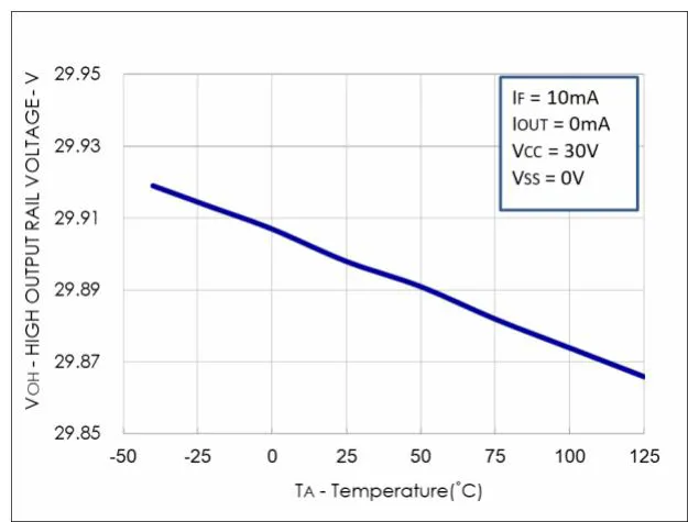
Fig.1 High output rail voltage vs. Temperature
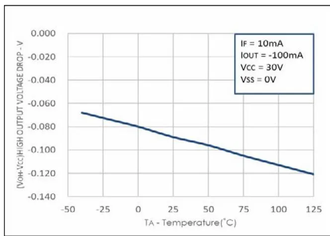
Fig.2 VoH vs. Temperature
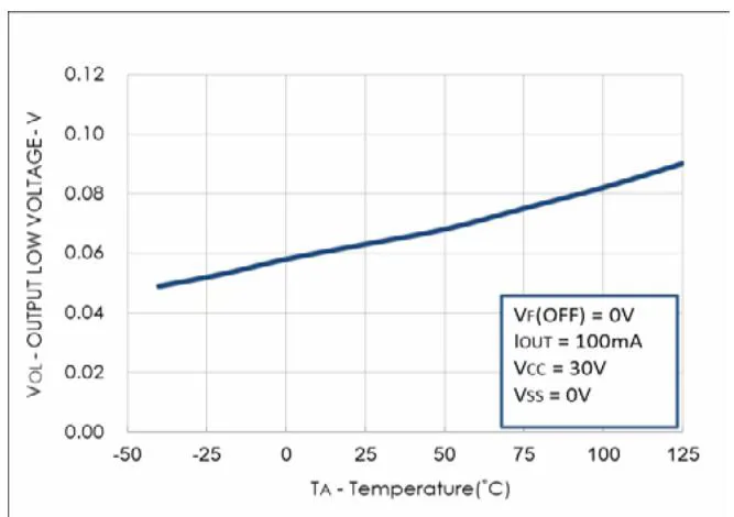
Fig.3 Vol vs. Temperature
Fig.5 Icc vs. Vcc
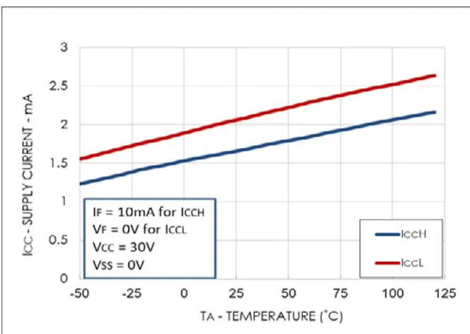
Fig.4 lcc vs. Temperature
Fig.6 IFLH vs. Hysteresis
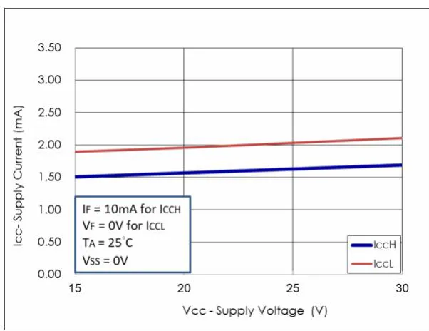
Fig.7 IFH vs. Temperature
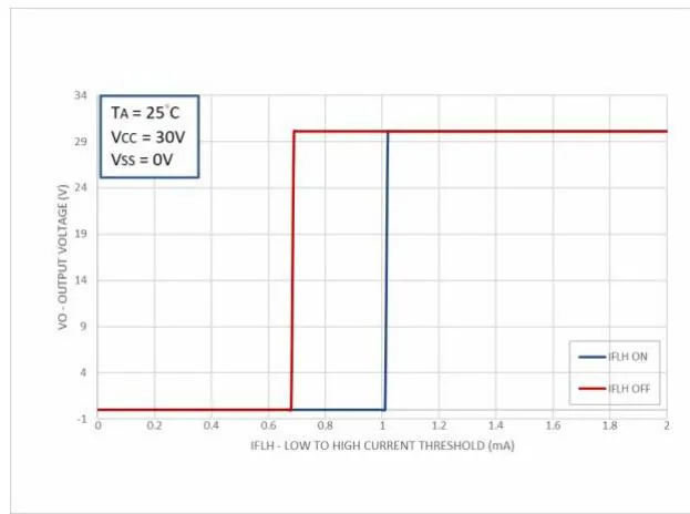
Fig.8 Propagation Delays vs. Vcc
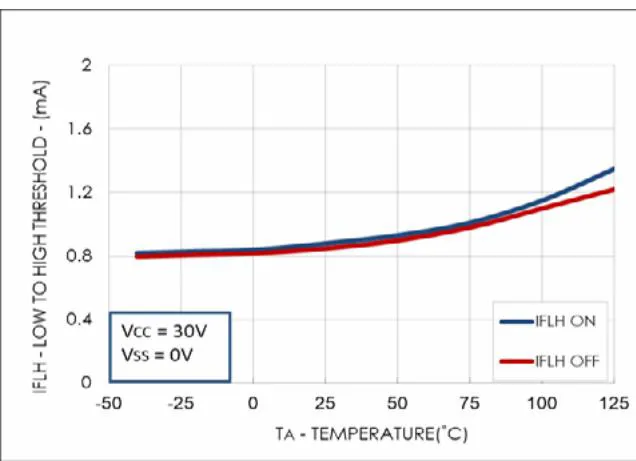
Fig.9 Propagation Delays vs. IF
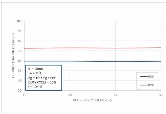
Fig.10 Propagation Delays vs. Temperature
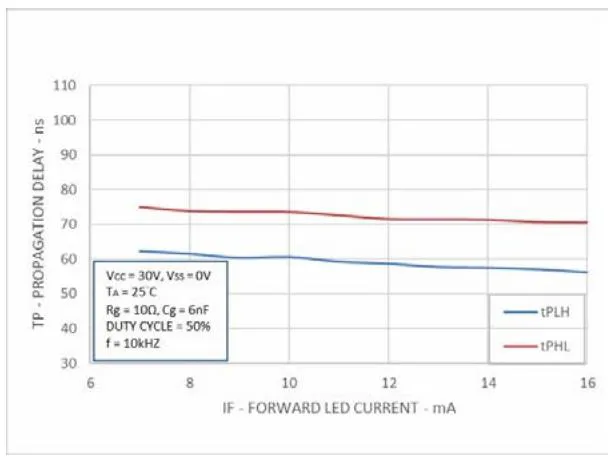
Fig.11 Propagation Delays vs. Rg
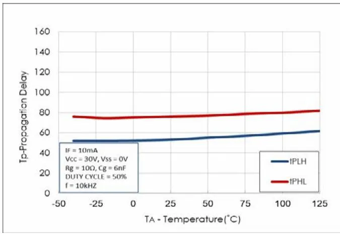
Fig.12 Propagation Delays vs. Cg
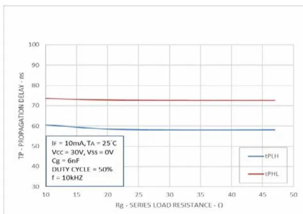
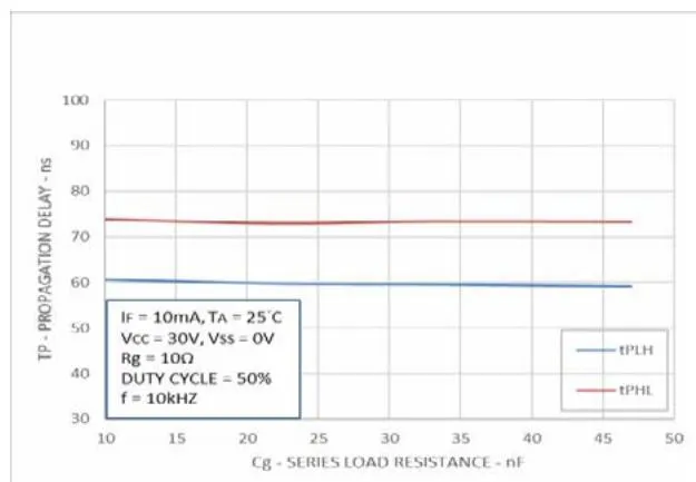
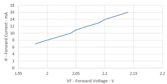
Fig.13 Input Current vs. Forward Voltage
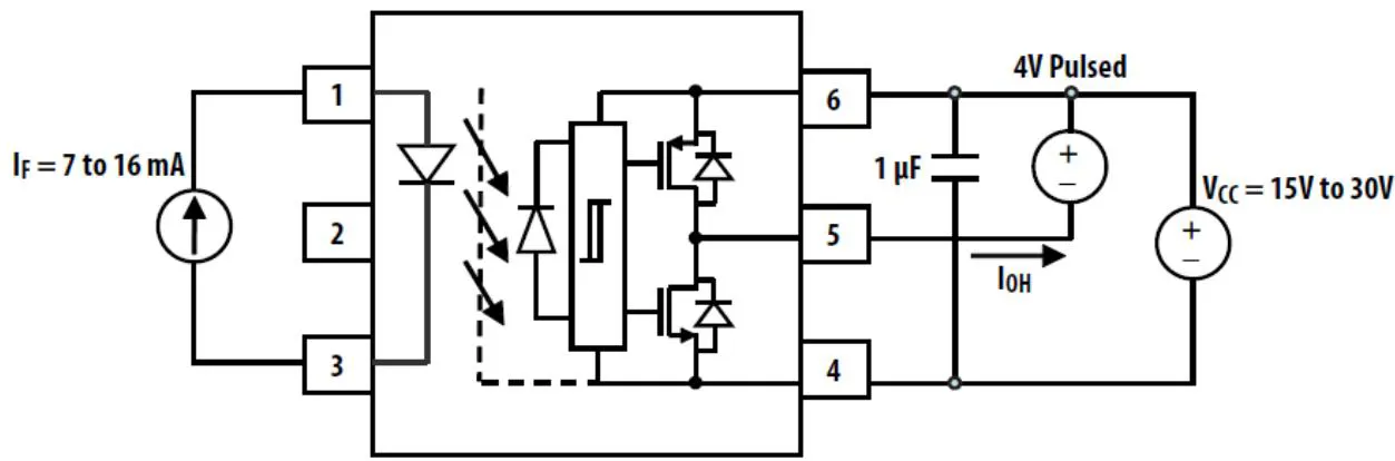
Fig.14 IOH Test Circuit
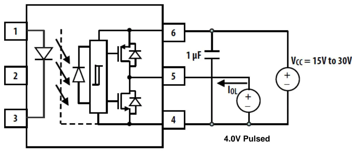
Fig.15 IOL Test Circuit
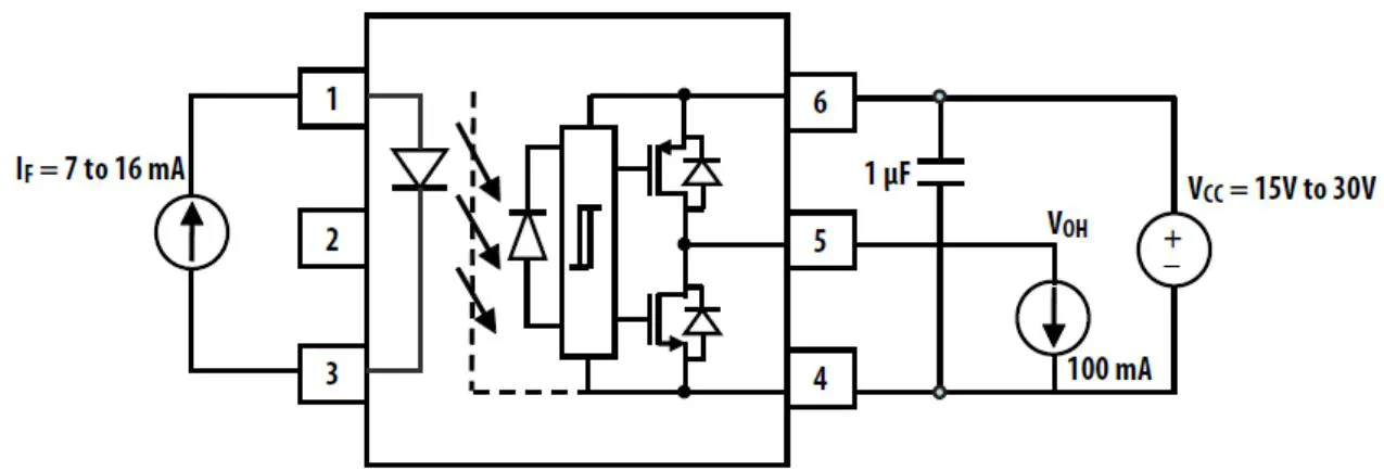
Fig.16 Test Circuit
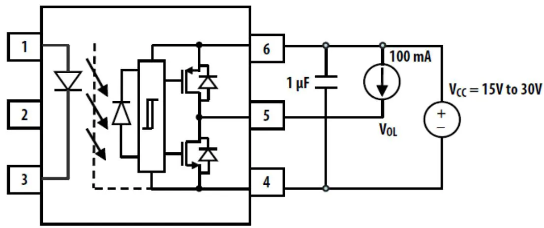
Fig.17 Vol Test Circuit
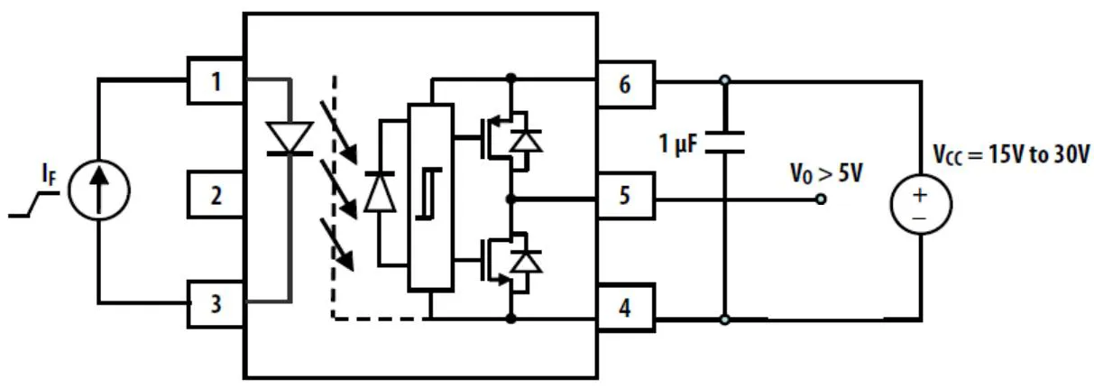
Fig.18 IFLH Test Circuit
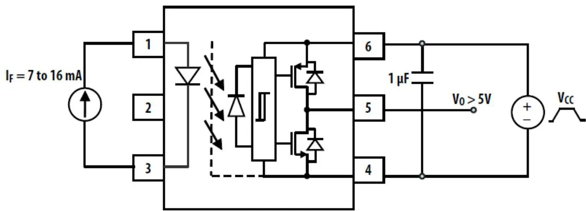
Fig.19 UVLO Test Circuit
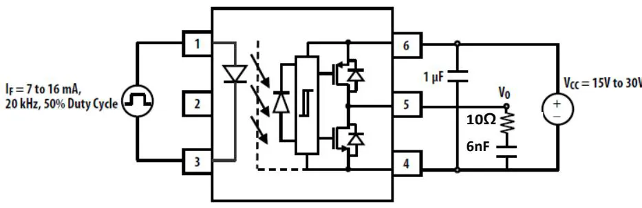
Fig.20 tPHL, tPLH, tr and tf Test Circuit and Waveforms
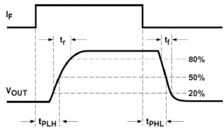
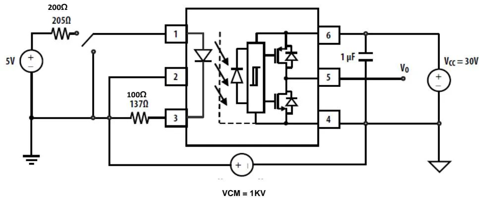
Fig.21 CMR Test Circuit with Split Resistors Network and Waveforms
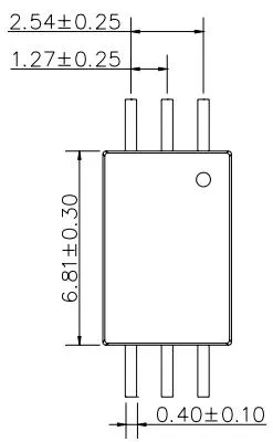
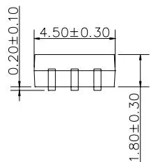
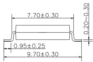
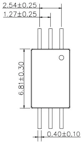
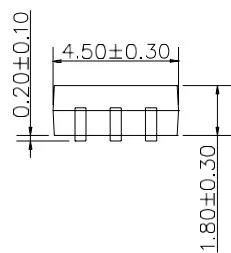
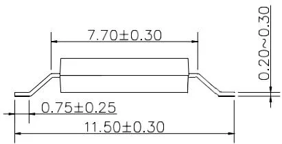
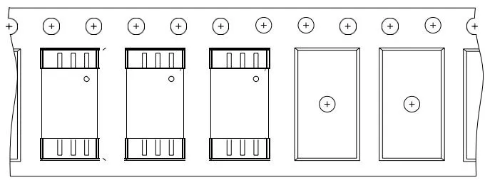
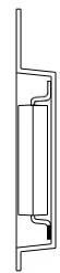
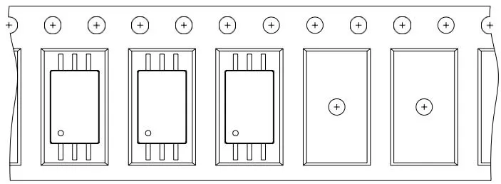
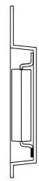
封装尺寸 (除非另有说明,尺寸单位均为毫米)
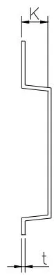
表面贴装引脚成形
SL 型(封装)尺寸
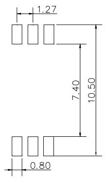
SLM 型(封装)尺寸
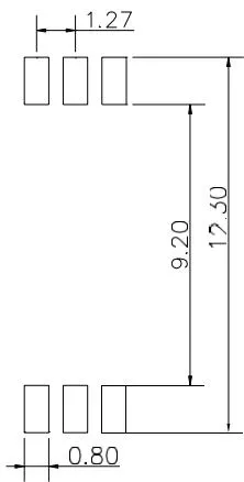
卷带包装尺寸(除非另有说明,尺寸单位均为毫米)
SL 型封装的卷带尺寸
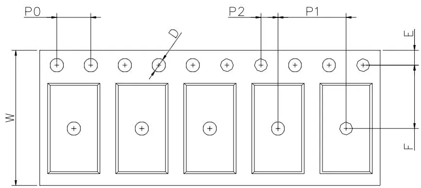
| Dimension Symbol | D | E | F | P0 | P1 | P2 | t | W | K |
| Dimension (mm) | 1.5±0.1 | 1.75±0.1 | 7.5±0.1 | 4.0±0.1 | 8.0±0.1 | 2.0±0.1 | 0.3±0.1 | 16.0±0.3 | 2.15±0.1 |
磁带与卷轴包装 规格
Option T1
Option T2
标记信息
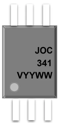
JOC : Company Abbr.
341 : Part Number & Rank
V : VDE Option
Y : Fiscal Year
Y : Manufacturing Code
WW : Work Week
JOC341订购信息
JOC341(Y)(Z)-GV
JOC- Company Abbr.
341 – Part Number
Y – Lead Form Option
Z - Tape and Reel Option (T1/T2)
G - Green
V – VDE Option (V or None)