
制造商
厂商型号
封装
规格书
描述
JMSH1001NS规格参数 |
|||
|---|---|---|---|
| Type | 中压MOSFET | ||
| RoHS | |||
| 制造商 | JJM | ||
| 类型 | N | ||
| VDS_Max/V | 100 | ||
| ID_Max /A | 308 | ||
| VGS(th)Typ/V | 3 | ||
| RDS(ON)Typ (mΩ)@VGS 10V | 1.9 | ||
| RDS(ON)Max (mΩ)@VGS 10V | 2.2 | ||
| RDS(ON)Typ (mΩ)@VGS 4.5V | |||
| RDS(ON)Max (mΩ)@VGS 4.5V | |||
| VGS_Max/V | ±20 | ||
JMSH1001NS详情
100V 1.9mΩ N沟道功率MOSFET JMSH1001NS
JMSH1001NS特色
超低速
低栅极电荷
100%UIS测试,100%RG测试
-
无铅铅镀层
-
无卤素且符合RoHS标准
Product Summary
| Parameter | Value | Unit |
| VDS | 100 | V |
| VGS(th)_Typ | 3.0 | V |
| ID (@ VGS = 10V) (1) | 308 | A |
| RDS(ON)_Typ (@ VGS = 10V) | 1.9 | mΩ |
JMSH1001NS应用
- 电动工具、电动车、机器人中的电动车驾驶
- DC/DC 及 AC/DC(SR)子系统的当前切换
- 电信中的电力管理,工业自动化,计算机工程
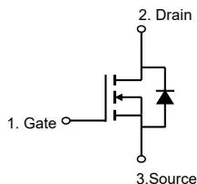
TO-247-3L Top View

TO-247-3L Bottom View

JMSH1001NS 订购信息
| Device | Package | # of Pins | Marking | MSL | TJ(°C) | Media | Quantity (pcs) |
| JMSH1001NS-U | TO-247-3L | 3 | SH1001N | NA | -55 to 150 | Tube | 30 |
JMSH1001NS 绝对最大额定值 (@ unless otherwise specified)
| Parameter | Symbol | Value | Unit | |
| Drain-to-Source Voltage | VDS | 100 | V | |
| Gate-to-Source Voltage | VGS | ±20 | V | |
| Continuous Drain Current (1) | TC=25°C | ID | 308 | A |
| TC=100°C | 195 | |||
| Pulsed Drain Current (2) | IDM | 537 | A | |
| Avalanche Energy (3) | EAS | 1838 | mJ | |
| Power Dissipation (4) | TC=25°C | PD | 367 | W |
| TC=100°C | 147 | |||
| Junction & Storage Temperature Range | TJ, TSTG | -55 to 150 | °C | |
vs.
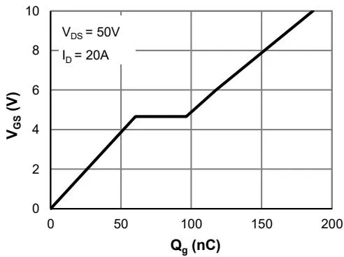
Gate Charge
JMSH1001NS 电气特性(@ unless otherwise specified)
| Parameter | Symbol | Conditions | Min. | Typ. | Max. | Unit | |
| STATIC PARAMETERS | |||||||
| Drain-Source Breakdown Voltage | V(BR)DSS | ID=250μA, VGS=0V | 100 | V | |||
| Zero Gate Voltage Drain Current | IDSS | VDS=80V, VGS=0V | 1.0 | μA | |||
| TJ=55°C | 5.0 | ||||||
| Gate-Body Leakage Current | IGSS | VDS=0V, VGS=±20V | ±100 | nA | |||
| Gate Threshold Voltage | VGS(th) | VDS=VGS, ID=250μA | 2.0 | 3.0 | 4.0 | V | |
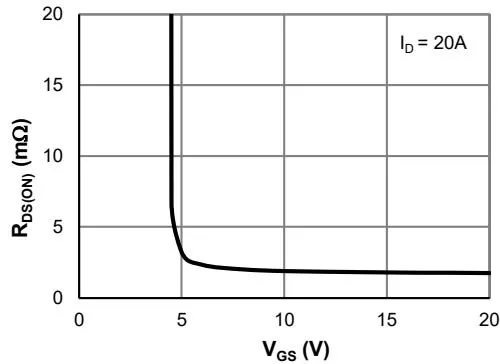
| Static Drain-Source ON-Resistance | RDS(ON) | VGS=10V, ID=20A | 1.9 | 2.2 | mΩ | ||
| Forward Transconductance | gFS | VDS=5V, ID=20A | 66 | S | |||
| Diode Forward Voltage | VSD | IS=1A, VGS=0V | 0.66 | 1.0 | V | ||
| Diode Continuous Current | IS | TC=25°C | 308 | A | |||
JMSH1001NS 动态参数 (5)
| Input Capacitance | Ciss | VGS=0V, VDS=50V, f=1MHz | 13489 | pF | ||
| Output Capacitance | Coss | 2166 | pF | |||
| Reverse Transfer Capacitance | Crss | 37 | pF | |||
| Gate Resistance | Rg | VGS=0V, VDS=0V, f=1MHz | 3.4 | Ω |
JMSH1001NS 切换参数 (5)
| Total Gate Charge (@ VGS = 10V) | Qg | VGS= 0 to 10V VDS= 50V, ID= 20A | 186 | nC | ||
| Total Gate Charge (@ VGS = 6.0V) | Qg | 118 | nC | |||
| Gate Source Charge | Qgs | 60 | nC | |||
| Gate Drain Charge | Qgd | 36 | nC | |||
| Turn-On DelayTime | tD(on) | VGS= 10V, VDS= 50V RL= 2.5Ω, RGEN= 3Ω | 41 | ns | ||
| Turn-On Rise Time | tr | 62 | ns | |||
| Turn-Off DelayTime | tD(off) | 133 | ns | |||
| Turn-Off Fall Time | tf | 75 | ns | |||
| Body Diode Reverse Recovery Time | trr | IF= 20A, dIF/dt= 100A/μs | 115 | ns | ||
| Body Diode Reverse Recovery Charge | Qrr | IF= 20A, dIF/dt= 100A/μs | 333 | nC |
JMSH1001NS 热性能参数
| Parameter | Symbol | Typ. | Max. | Unit |
| Thermal Resistance, Junction-to-Ambient | RθJA | 48 | 58 | °C/W |
| Thermal Resistance, Junction-to-Case | RθJC | 0.34 | 0.41 | °C/W |
备注:
-
Computed continuous current assumes the condition of while the actual continuous current depends on the thermal & electro-mechanical application board design.
-
This single-pulse measurement was taken under .
-
of 1838 mJ is based on starting , , , , ; 100% test at , .
-
The power dissipation is based on .
-
This value is guaranteed by design hence it is not included in the production test.
JMSH1001NS 典型电气与热特性
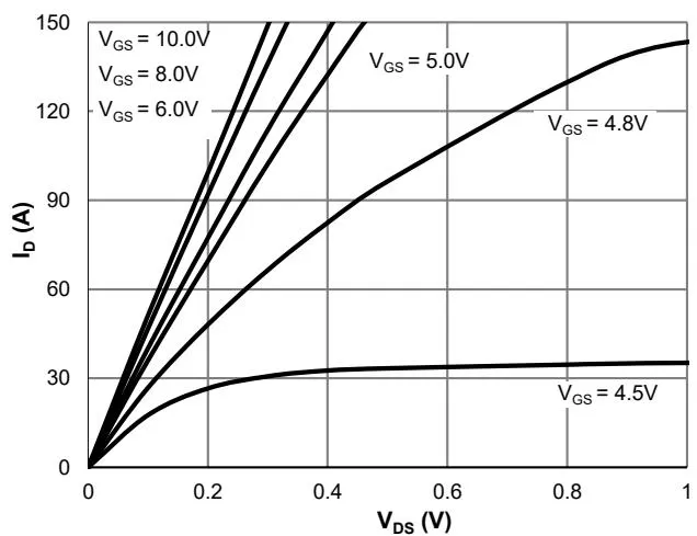
Figure 1: Saturation Characteristics
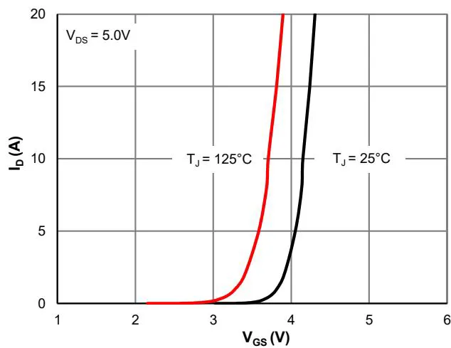
Figure 2: Transfer Characteristics
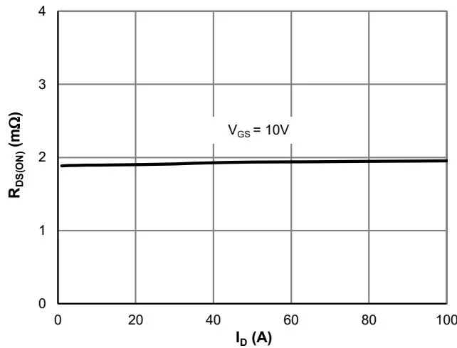
Figure 3: vs. Drain Current
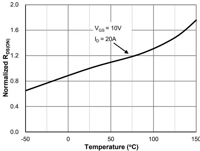
Figure 4: vs. Junction Temperature
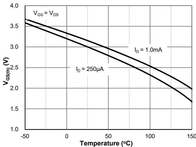
Figure 5: vs. Junction Temperature
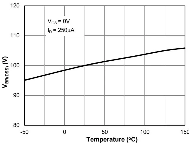
Figure 6: vs. Junction Temperature
Typical Electrical & Thermal Characteristics
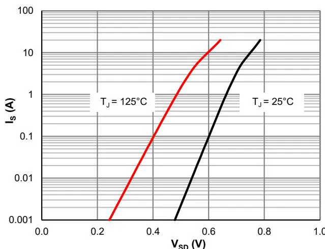
Figure 7: Body-Diode Characteristics
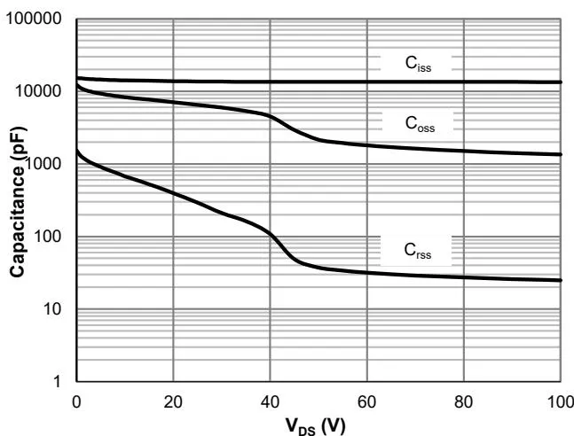
Figure 8: Capacitance Characteristics
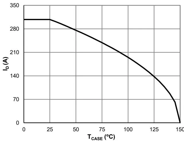
Figure 9: Current De-rating
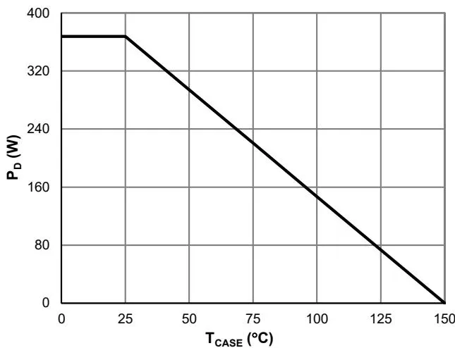
Figure 10: Power De-rating
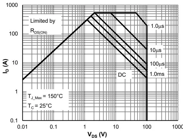
Figure 11: Maximum Safe Operating Area
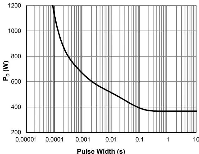
Figure 12: Single Pulse Power Rating, Junction-to-Case
Typical Electrical & Thermal Characteristics
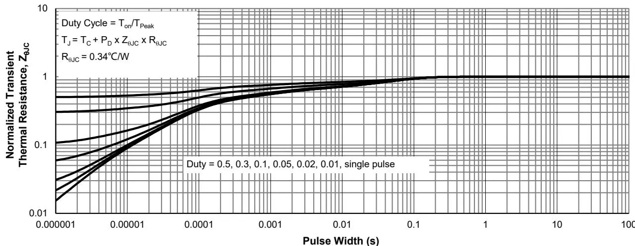
Figure 13: Normalized Maximum Transient Thermal Impedance
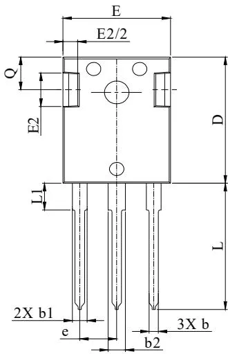
TO-247-3L 封装信息
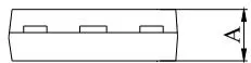
Type_A Package Outline
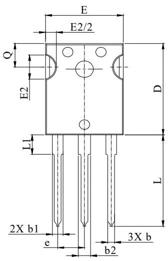
| DIM. | MILLIMETER | ||
| MIN. | NOM. | MAX. | |
| A | 4.80 | 5.02 | 5.21 |
| b | 1.00 | 1.20 | 1.40 |
| b1 | 1.90 | 2.00 | 2.39 |
| b2 | 2.87 | 3.00 | 3.22 |
| c | 0.41 | 0.60 | 0.79 |
| D | 20.80 | 21.00 | 21.20 |
| E | 15.50 | 15.94 | 16.13 |
| E2 | 4.32 | 5.49 | |
| L | 19.70 | 20.07 | 20.32 |
| L1 | 4.00 | 4.40 | |
| K | 2.20 | 2.50 | |
| e | 5.44 BSC | ||
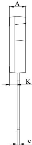
Type_B Package Outline
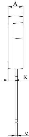
| DIM. | MILLIMETER | ||
| MIN. | NOM. | MAX. | |
| A | 4.80 | 5.02 | 5.21 |
| b | 1.00 | 1.20 | 1.40 |
| b1 | 1.90 | 2.00 | 2.39 |
| b2 | 2.87 | 3.00 | 3.22 |
| c | 0.41 | 0.60 | 0.79 |
| D | 20.80 | 21.00 | 21.20 |
| E | 15.50 | 15.94 | 16.13 |
| E2 | 4.32 | 5.49 | |
| L | 19.70 | 20.07 | 20.32 |
| L1 | 4.00 | 4.40 | |
| K | 2.20 | 2.50 | |
| e | 5.44 BSC | ||