制造商
厂商型号
封装
规格书
描述
JMSH0403PGQ规格参数 |
|||
|---|---|---|---|
| Type | 汽车MOSFET | ||
| RoHS | |||
| 制造商 | JJM | ||
| 类型 | N | ||
| VDS_Max/V | 40 | ||
| ID_Max /A | 137 | ||
| VGS(th)Typ/V | 2.8 | ||
| RDS(ON)Typ (mΩ)@ VGS 10V | 2.8 | ||
| RDS(ON)Max (mΩ)@ VGS 10V | 3.7 | ||
| VGS_Max/V | ±20 | ||
JMSH0403PGQ详情
40伏,137安培,2.8mΩ N通道功率SGT MOSFET JMSH0403PGQ
JMSH0403PGQ特点
- 超低导通电阻,
- 低栅极电荷
- 100% UIS测试
- 100% ΔVds测试
- 无卤素;符合RoHS
- AEC-Q101 合格
JMSH0403PGQ应用
- 负载开关
- PWM应用
- 通用汽车应用
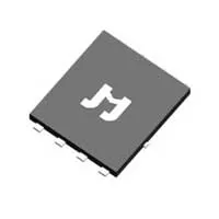
PDFN5X6-8L
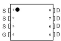
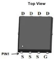
Pin
产品摘要
| Parameters | Value | Unit |
| VDSS | 40 | V |
| VGS(th)_Typ | 2.8 | V |
| ID(@VGS=10V) | 137 | A |
| RDS(ON)_Typ(@VGS=10V) | 2.8 | mΩ |

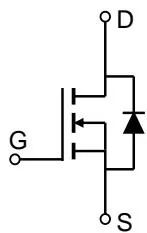
Schematic Diagram
JMSH0403PGQ订购信息
| Device | Marking | MSL | Form | Package | Reel(pcs) | Per Carton (pcs) |
| JMSH0403PGQ-13 | SH0403PQ | 1 | Tape&Reel | PDFN5x6-8L | 5000 | 50000 |
Absolute Maximum Ratings (@ unless otherwise specified)
| Symbol | Parameter | Value | Unit | |
| VDS | Drain-to-Source Voltage | 40 | V | |
| VGS | Gate-to-Source Voltage | ±20 | V | |
| ID | Continuous Drain Current | TC=25°C | 137 | A |
| TC=100°C | 97 | |||
| IDM | Pulsed Drain Current (1) | Refer to Fig.4 | A | |
| EAS | Single Pulsed Avalanche Energy (2) | 212 | mJ | |
| PD | Power Dissipation | TC=25°C | 125 | W |
| TC=100°C | 63 | |||
| TJ, TSTG | Junction & Storage Temperature Range | -55 to 175 | °C | |
JMSH0403PGQ热特性
| Symbol | Parameter | Max | Unit |
| RθJA | Thermal Resistance, Junction to Ambient(3) | 43 | °C/W |
| RθJC | Thermal Resistance, Junction to Case | 1.2 |
JMSH0403PGQ电子特性 unless otherwise specified)
| Symbol | Parameter | Conditions | Min. | Typ. | Max. | Unit |
| Off Characteristics | ||||||
| V(BR)DSS | Drain-Source Breakdown Voltage | ID=250μA, VGS=0V | 40 | - | - | V |
| IDSS | Zero Gate Voltage Drain Current | VDS=32V, VGS=0V | - | - | 1.0 | μA |
| IGSS | Gate-Body Leakage Current | VDS=0V, VGS=±20V | - | - | ±100 | nA |
| On Characteristics | ||||||
| VGS(th) | Gate Threshold Voltage | VDS=VGS, ID=250μA | 2.0 | 2.8 | 3.7 | V |
| RDS(ON) | Static Drain-Source ON-Resistance(4) | VGS=10V, ID=20A | - | 2.8 | 3.7 | mΩ |
| Dynamic Characteristics | ||||||
| Rg | Gate Resistance | f=1MHz | - | 0.7 | - | Ω |
| Ciss | Input Capacitance | VGS=0V, VDS=20V, f=1MHz | 1398 | 1958 | 2643 | pF |
| Coss | Output Capacitance | 890 | 1246 | 1682 | pF | |
| Crss | Reverse Transfer Capacitance | 65 | 91 | 123 | pF | |
| Qg | Total Gate Charge | VGS=0 to 10VVDS=20V, ID=20A | 22 | 30 | 41 | nC |
| Qgs | Gate Source Charge | - | 10 | - | nC | |
| Qgd | Gate Drain("Miller") Charge | - | 8 | - | nC | |
| Switching Characteristics | ||||||
| td(on) | Turn-On DelayTime | VGS=10V, VDD=20VID=20A, RGEN=3Ω | - | 13 | - | ns |
| tr | Turn-On Rise Time | - | 28 | - | ns | |
| td(off) | Turn-Off DelayTime | - | 21 | - | ns | |
| tf | Turn-Off Fall Time | - | 8 | - | ns | |
| Body Diode Characteristics | ||||||
| IS | Maximum Continuous Body Diode Forward Current | - | - | 137 | A | |
| ISM | Maximum Pulsed Body Diode Forward Current | - | - | 550 | A | |
| VSD | Body Diode Forward Voltage | VGS=0V, IS=20A | - | 1.2 | V | |
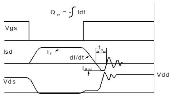
| trr | Body Diode Reverse Recovery Time | IF=20A, di/dt=100A/us | 27 | 38 | 52 | ns |
| Qrr | Body Diode Reverse Recovery Charge | - | 35 | - | nC | |
Notes: 1. Repetitive Rating: Pulse Width Limited by Maximum Junction Temperature.
2. condition: Starting , , , , , , during time in avalanche.
3. is measured with the device mounted on a 1inch² pad of 2oz copper FR4 PCB.
4. Pulse Test: Pulse Width Duty Cycle
典型表现 特征
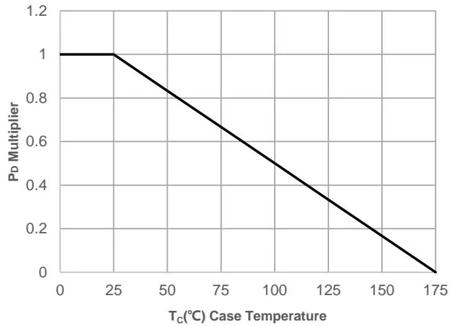
Figure 1: Power De-rating
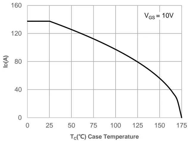
Figure 2: Current De-rating
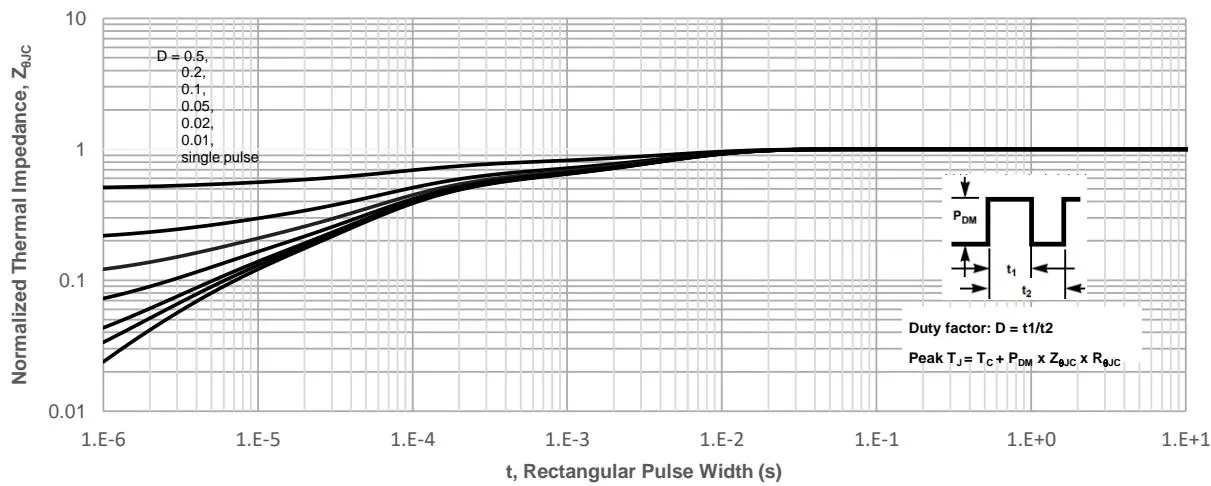
Figure 3: Normalized Maximum Transient Thermal Impedance
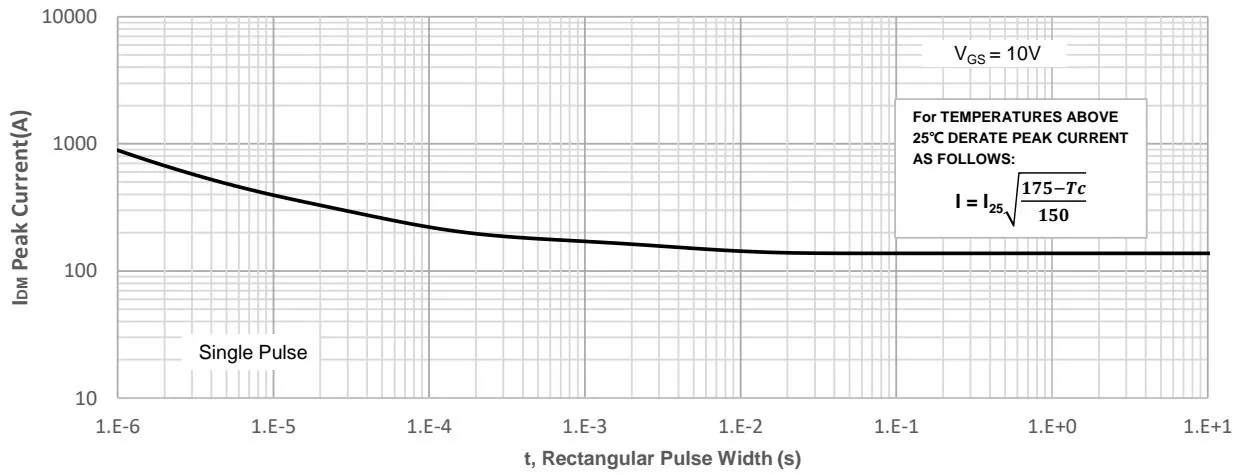
Figure 4: Peak Current Capacity
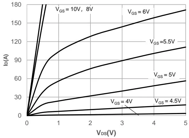
Figure 5: Output Characteristics
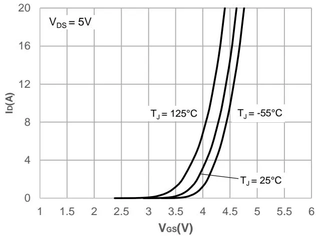
Figure 6: Typical Transfer Characteristics
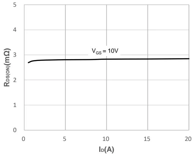
Figure 7: On-resistance vs. Drain Current
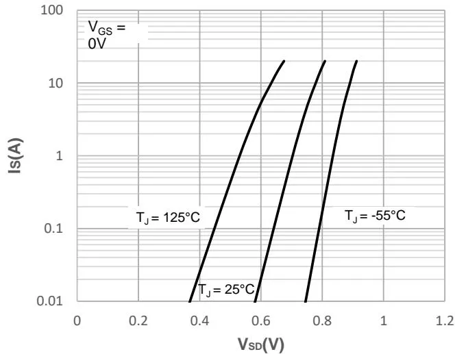
Figure 8: Body Diode Characteristics
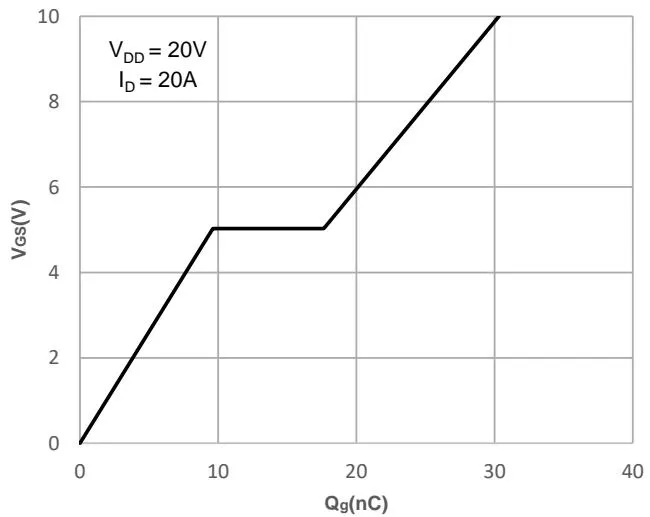
Figure 9: Gate Charge Characteristics
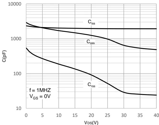
Figure 10: Capacitance Characteristics
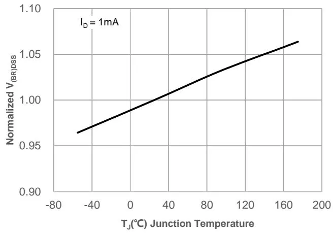
Figure 11: Normalized Breakdown voltage vs. Junction Temperature
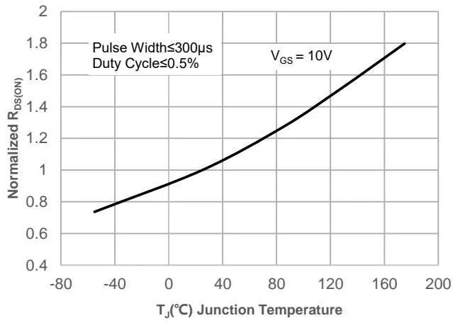
Figure 12: Normalized on Resistance vs. Junction Temperature
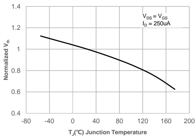
Figure 13: Normalized Threshold Voltage vs. Junction Temperature
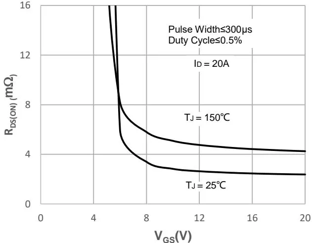
Figure 14: vs.
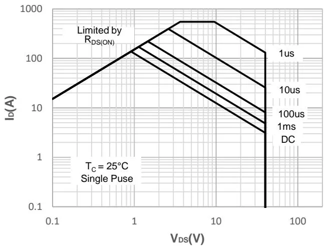
Figure 15: Maximum Safe Operating Area
JMSH0403PGQ 测试电路
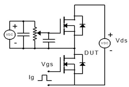
Figure 1: Gate Charge Test Circuit & Waveform
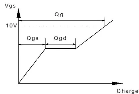
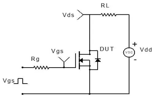
Figure 2: Resistive Switching Test Circuit & Waveform
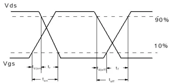
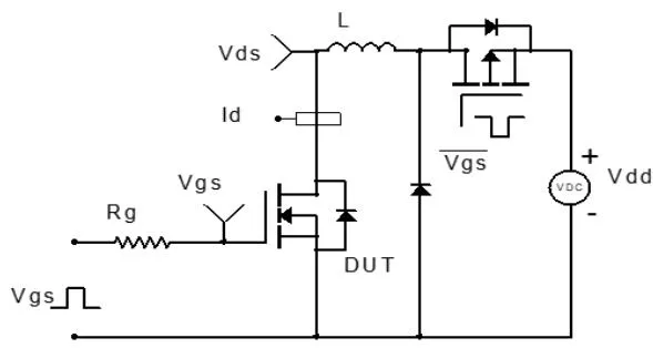
Figure 3: Unclamped Inductive Switching Test Circuit& Waveform
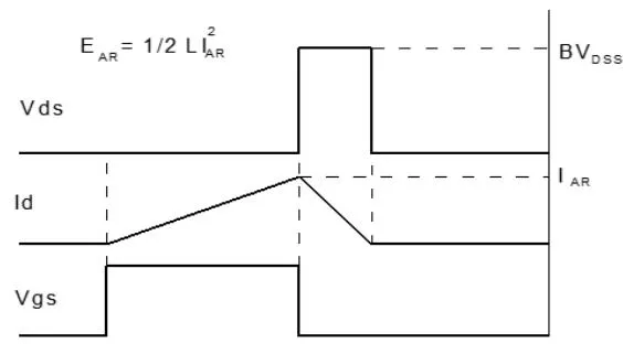
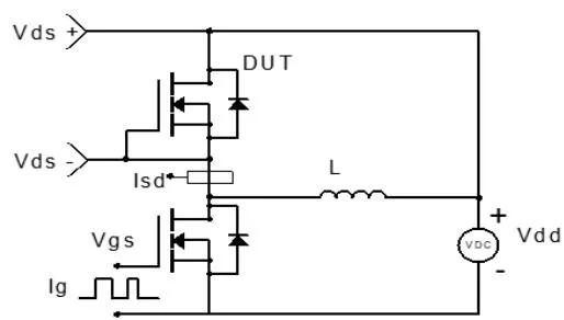
Figure 4: Diode Recovery Test Circuit & Waveform
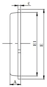
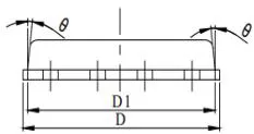
机械封装 数据(PDFN5X6-8L)
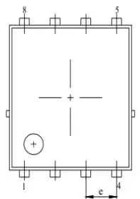
Package Outline
Top View
Side View
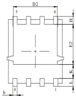
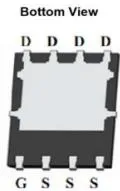
Bottom View
Front View
备注
- Dimension and tolerance per ASME Y14.5M, 1994.
- All dimensions in millimeter (angle in degree).
- Dimensions D1 and E1 do not include mold flash protrusions or gate burrs.
| DIM. | MILLIMETER | ||
| MIN. | NOM. | MAX. | |
| A | 0.9 | 1 | 1.15 |
| b | 0.31 | 0.41 | 0.51 |
| C | 0.24 | 0.32 | 0.4 |
| D | 5 | 5.2 | 5.4 |
| D1 | 4.95 | 5.05 | 5.15 |
| D2 | 4 | 4.1 | 4.2 |
| E | 6.05 | 6.15 | 6.25 |
| E1 | 5.5 | 5.6 | 5.7 |
| E2 | 3.42 | 3.53 | 3.63 |
| e | 1.2TBSC | ||
| H | 0.6 | 0.7 | 0.8 |
| L | 0.5 | 0.7 | 0.8 |
| K | 1.23 REF | ||
| 0 | 10 | ||
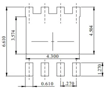
Recommended Soldering Footprint
DIMENSIONS:MILLIMETERS