
JMH65R090PTLFD规格参数 |
|||
|---|---|---|---|
| Type | 高压MOSFET | ||
| RoHS | |||
| 制造商 | JJM | ||
| 类型 | N | ||
| VDS_Max/V | 650 | ||
| ID_Max/A | 24 | ||
| VGS(th)Typ/V | 3.3 | ||
| RDS(ON)Typ (mΩ) @VGS 10V | 80 | ||
| RDS(ON)_Max (mΩ) @VGS 10V | 90 | ||
| VGS_Max (V) | ±30 | ||
JMH65R090PTLFD详情
650V,24A,80mΩ N沟道功率超级结场效应晶体管 JMH65R090PTLFD
特点
- 优秀的以及低栅极电荷
- 100%通过UIS测试
- 检测率为100%的ΔVds
- 无卤素;符合RoHS
JMH65R090PTLFD应用
- 与PFC的SMPS
- 反激式拓扑与LLC拓扑
- 银牌ATX电源、适配器、电视、照明、电信设备
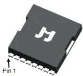
PowerJE®10x12
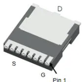
Pin Assignment
Product Summary
| Parameters | Value | Unit |
| VDSS | 650 | V |
| VGS(th)_Typ | 3.3 | V |
| ID(@VGS=10V) | 24 | A |
| RDS(ON)_Typ(@VGS=10V) | 80 | mΩ |
RoHS

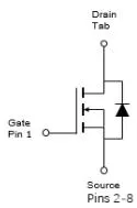
Schematic Diagram
订购信息
| Device | Marking | MSL | Form | Package | Reel(pcs) | Per Carton (pcs) |
| JMH65R090PTLFD-13 | H65R090PF | 1 | Tape&Reel | PowerJE®10x12 | 2000 | 10000 |
Absolute Maximum Ratings (@ unless otherwise specified)
| Symbol | Parameter | Value | Unit | |
| VDS | Drain-to-Source Voltage | 650 | V | |
| VGS | Gate-to-Source Voltage | ±30 | V | |
| ID | Continuous Drain Current | TC=25°C | 24 | A |
| TC=100°C | 15 | |||
| IDM | Pulsed Drain Current (1) | Refer to Fig.4 | A | |
| EAS | Single Pulsed Avalanche Energy (2) | 414 | mJ | |
| PD | Power Dissipation | TC=25°C | 135 | W |
| TC=100°C | 54 | |||
| TJ, TSTG | Junction & Storage Temperature Range | -55 to 150 | °C | |
Thermal Characteristics
| Symbol | Parameter | Max | Unit |
| RθJA | Thermal Resistance, Junction to Ambient(3) | 35 | °C/W |
| RθJC | Thermal Resistance, Junction to Case | 0.9 |
Electrical Characteristics unless otherwise specified)
| Symbol | Parameter | Conditions | Min. | Typ. | Max. | Unit |
| Off Characteristics | ||||||
| V(BR)DSS | Drain-Source Breakdown Voltage | ID=250μA, VGS=0V | 650 | - | - | V |
| IDSS | Zero Gate Voltage Drain Current | VDS=650V, VGS=0V | - | - | 10.0 | μA |
| IGSS | Gate-Body Leakage Current | VDS=0V, VGS=±30V | - | - | ±100 | nA |
| On Characteristics | ||||||
| VGS(th) | Gate Threshold Voltage | VDS=VGS, ID=250μA | 2.3 | 3.3 | 4.3 | V |
| RDS(ON) | Static Drain-Source ON-Resistance(4) | VGS=10V, ID=10A | - | 80 | 90 | mΩ |
| Dynamic Characteristics | ||||||
| Rg | Gate Resistance | f=1MHz | - | 3.3 | - | Ω |
| Ciss | Input Capacitance | VGS=0V, VDS=325V, f=1MHz | 1995 | 2793 | 3771 | pF |
| Coss | Output Capacitance | 46 | 64 | 86 | pF | |
| Crss | Reverse Transfer Capacitance | - | 6.8 | - | pF | |
| Qg | Total Gate Charge | VGS=0 to 10V VDS=325V, ID=20A | 41 | 58 | 78 | nC |
| Qgs | Gate Source Charge | 15 | 20 | 27 | nC | |
| Qgd | Gate Drain("Miller") Charge | 16 | 22 | 29 | nC | |
| Switching Characteristics | ||||||
| td(on) | Turn-On DelayTime | VGS=10V, VDD=325V ID=20A, RGEN=24Ω | - | 66 | - | ns |
| tr | Turn-On Rise Time | - | 67 | - | ns | |
| td(off) | Turn-Off DelayTime | - | 155 | - | ns | |
| tf | Turn-Off Fall Time | - | 45 | - | ns | |
| Body Diode Characteristics | ||||||
| IS | Maximum Continuous Body Diode Forward Current | - | - | 24 | A | |
| ISM | Maximum Pulsed Body Diode Forward Current | - | - | 95 | A | |
| VSD | Body Diode Forward Voltage | VGS=0V, IS=20A | - | 1.2 | V | |
| trr | Body Diode Reverse Recovery Time | IF=20A, di/dt=100A/us | 137 | 192 | 259 | ns |
| Qrr | Body Diode Reverse Recovery Charge | - | 1230 | - | nC | |
Notes: 1. Repetitive Rating: Pulse Width Limited by Maximum Junction Temperature.
-
condition: Starting , , , , , , during time in avalanche.
-
is measured with the device mounted on FR-4 substrate PC board, 2oz copper, with minimum recommended pad layout.
-
Pulse Test: Pulse Width Duty Cycle
典型性能特性
Figure 1: Power De-rating
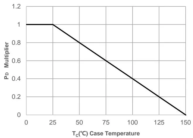
Figure 2: Current De-rating
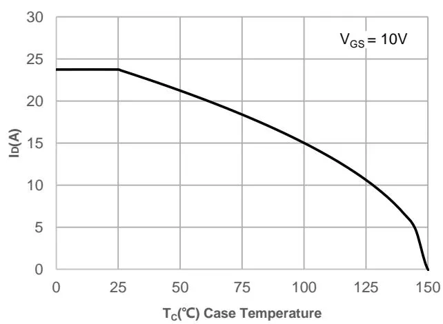
Figure 3: Normalized Maximum Transient Thermal Impedance
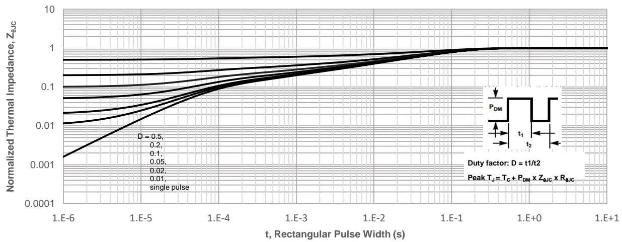
Figure 4: Peak Current Capacity
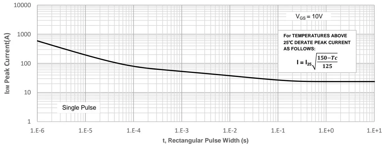
Figure 5: Output Characteristics
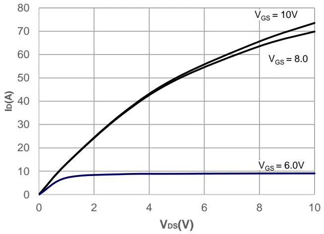
Figure 6: Typical Transfer Characteristics
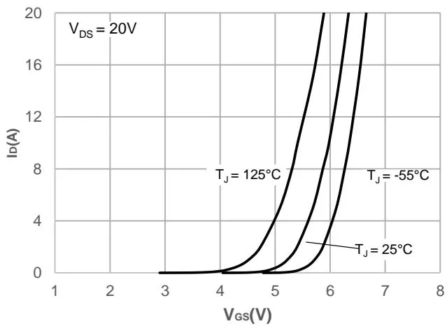
Figure 7: On-resistance vs. Drain Current
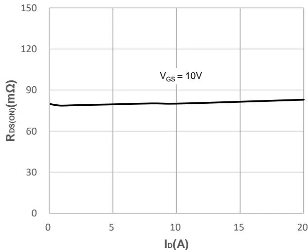
Figure 8: Body Diode Characteristics
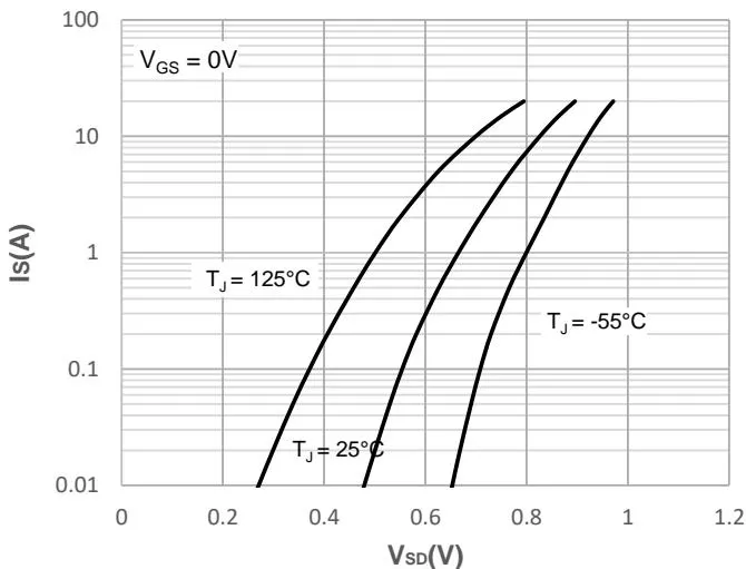
Figure 9: Gate Charge Characteristics
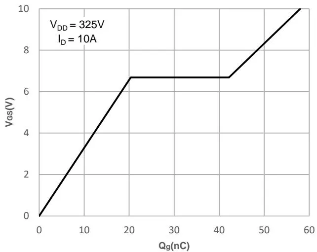
Figure 10: Capacitance Characteristics
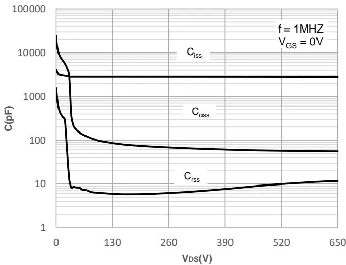
Figure 11: Normalized Breakdown voltage vs. Junction Temperature
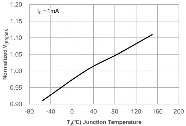
Figure 12: Normalized on Resistance vs. Junction Temperature
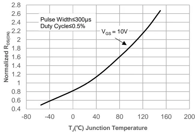
Figure 13: Normalized Threshold Voltage vs. Junction Temperature
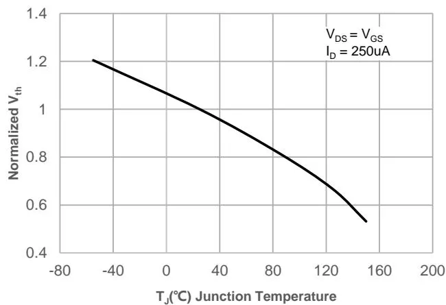
Figure 14: vs.
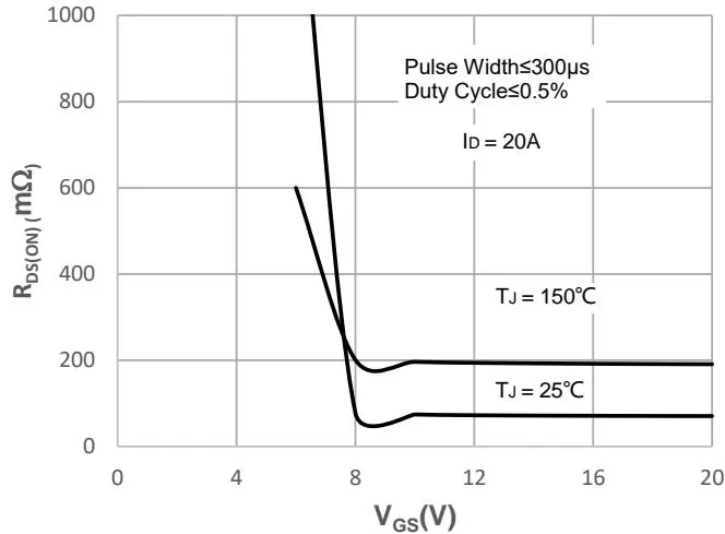
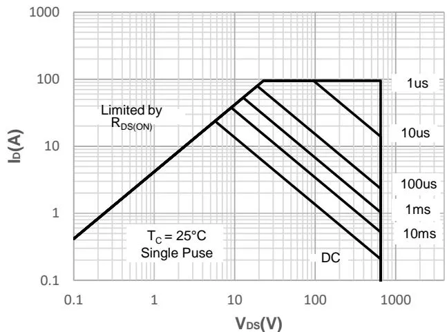
Figure 15: Maximum Safe Operating Area
测试电路
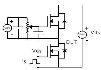
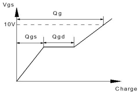
Figure 1: Gate Charge Test Circuit & Waveform
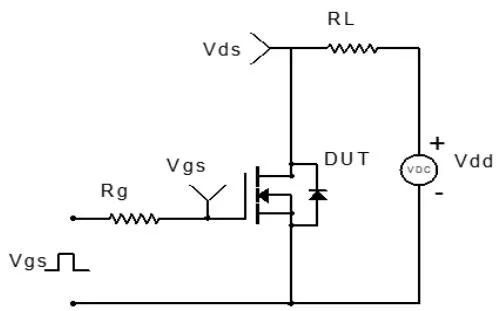
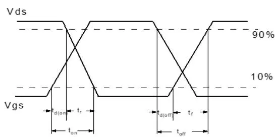
Figure 2: Resistive Switching Test Circuit & Waveform
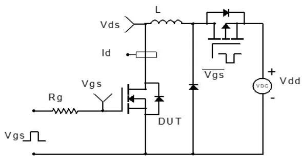
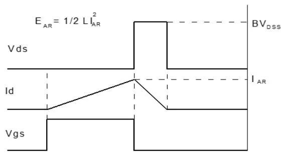
Figure 3: Unclamped Inductive Switching Test Circuit& Waveform
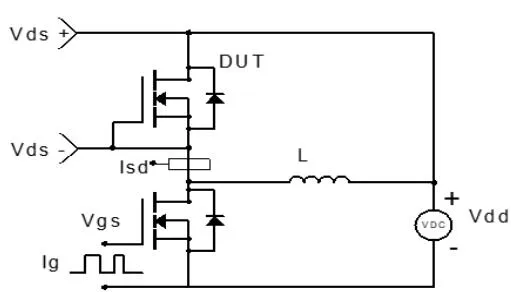
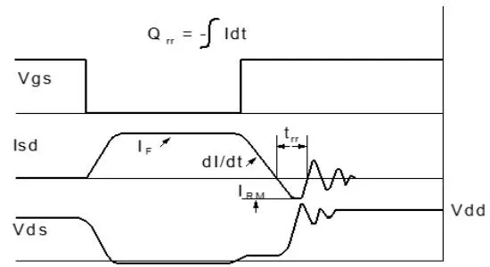
Figure 4: Diode Recovery Test Circuit & Waveform
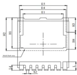
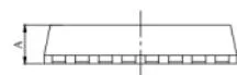
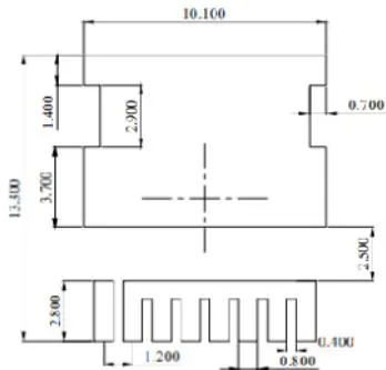
JMH65R090PTLFD封装机械数据(PowerJE®10x12)
Package Outlines
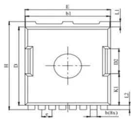
Top View
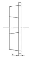
Side View
Bottom View
| DIM. | MILLIMETER | ||
| MIN | NOM | MAX | |
| A | 2.20 | 2.30 | 2.50 |
| b | 0.70 | 0.80 | 0.90 |
| b1 | 9.70 | 9.80 | 9.90 |
| b2 | 0.42 | 0.46 | 0.50 |
| C | 0.40 | 0.50 | 0.65 |
| D | 10.28 | 10.38 | 10.58 |
| D2 | 3.30 | ||
| E | 9.70 | 9.90 | 10.10 |
| E1 | 7.80 | ||
| E4 | 8.80 | ||
| E5 | 9.20 | ||
| e | 1.20(BSC) | ||
| H | 11.48 | 11.68 | 11.88 |
| HI | 6.55 | 6.75 | 6.85 |
| H2 | 7.30 | ||
| H3 | 3.20 | ||
| H4 | 3.80 | ||
| K1 | 4.18 | ||
| L | 1.70 | 1.90 | 2.10 |
| L1 | 0.70 | ||
| L2 | 0.60 | ||
| L4 | 1.00 | 1.15 | 1.30 |
Front View
Recommended Soldering Footprint
NOTES:
-
Dimension and tolerance per ASME Y14.5M, 1994.
-
All dimensions in millimeter.
-
Dimensions do not include burrs or mold flash. Mold flash or burrs does not exceed .
DIMENSIONS: MILIMETERS